Availability
Published
Product Code
MFR-1807-803
Product Item Code
HYN-H28S7Q302BMR-UFS
Device Manufacturer
Hynix
Device Type
NAND Flash
Subscription
Memory - NAND & DRAM
Channel
Memory - NAND Floorplan Analysis
SK Hynix H28S7Q302BMR-UFS 48L 3D-V3 NAND Flash (UFS2.1) Memory Functional Analysis
This report presents a Memory Functional Analysis of the SK Hynix H27DGLG die found inside the
SK Hynix H28S7Q302BMR-UFS package. The H28S7Q302BMR-UFS was extracted from the
Xiaomi Tech Mi 8 smartphone with the model number M1803E1A.
This report contains the following detailed information:
This report contains the following detailed information:
- Selected teardown photographs, package photographs, package X-rays, die markings, and die photographs
- SEM cross-sectional micrographs of a bevel through the memory array showing the active, BL and WL level plan-view features of the memory array and a cross section through the BL, showing the general structure of the flash cell array, die dielectric materials, major features, and transistors
- Measurements of vertical and horizontal dimensions of major microstructural features
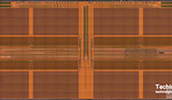
- Plan-view optical micrograph of the die delayered to diffusion layer
- Identification of major functional blocks on a diffusion layer die photograph
- Table of functional block sizes and percentage die utilization
- High-resolution top metal and diffusion level die photographs delivered in the CircuitVision software
![]()
The Authoritative Information Platform to the Semiconductor Industry.

