PFAS in Semiconductor Manufacturing: A Major Sustainability Challenge
Author: Carrie MacGillivray / February 29, 2024

As the speed of technological advancement continues to accelerate, the semiconductor industry plays a pivotal role as it helps propel innovations that shape our modern world. Yet, amid the development of the next generation of silicon chips and integrated circuits lies a silent challenge: the pervasive use of per- and polyfluoroalkyl substances (PFAS). These chemicals, renowned for their resistance to heat, water, and oil, have found their way into various industrial processes, including semiconductor manufacturing. But at what cost?
Being able to quantify the environmental impact is a difficult proposition for any manufacturer. TechInsights is tracking chemical usage and the implications in its Semiconductor Manufacturing Carbon Model. The model provides estimates on the amounts of chemicals that contain PFAS, including antireflective coating, photoresist, top-coat, and spin-on. This information is critical to inform the ecosystem of the opportunities and options that exist to reduce PFAS.
Platform Login Start My Free Trial
The Rise of PFAS
PFAS, a class of synthetic compounds, have garnered widespread attention because of their unique properties. These chemicals offer nonstick and heat-resistant qualities, making them indispensable in many industrial applications. From firefighting foams to nonstick cookware found in our kitchen cabinets, PFAS are present in many sectors, including the semiconductor industry.
In semiconductor manufacturing, PFAS play a crucial role in the production of integrated circuits. They are primarily utilized in the photolithography process, where intricate patterns are etched onto silicon wafers. Chemicals containing PFAS facilitate the smooth transfer of these patterns onto the semiconductor substrate, ensuring precise and reliable chip fabrication.
TechInsights’ Semiconductor Manufacturing Carbon Model quantifies the PFAS by technology node and fab across antireflective coating, photoresist, topcoat, and, in some cases, spin on. The amount of PFAS consumed in each technology node depends on the number of masks used and the complexity of the multipatterning steps. The manufacture of 10nm nodes involved optical lithography (also known as deep ultraviolet (DUV) lithography). In 2018, the introduction of extreme ultraviolet (EUV) lithography at 7nm meant that mask counts could be reduced, thus reducing PFAS-containing chemicals. However, as nodes continue to advance, the PFAS increase as the wafers become denser with more masks once again. It’s expected that when 2nm is introduced, and with the introduction of High NA (Numerical Aperture) EUV lithography, the PFAS chemical impact will once again wane. From a timing perspective, we expect this post-2025. If the past can indicate the future, chips produced by high-NA EUV will require ~10%–15% fewer masks (and less PFAS). The challenge will be preserving that rather than seeing it surge again. But, as these chips become more powerful and go beyond the inherent width of high-NA EUV, the number of masks will increase once again.
Figure 1 highlights the shift in consumption of chemicals containing PFAS from 28nm through to 14A+ and are representative of fabs that are producing these technology nodes. There was a 21.9% decrease in chemicals containing PFAS following the shift from DUV to EUV lithography.
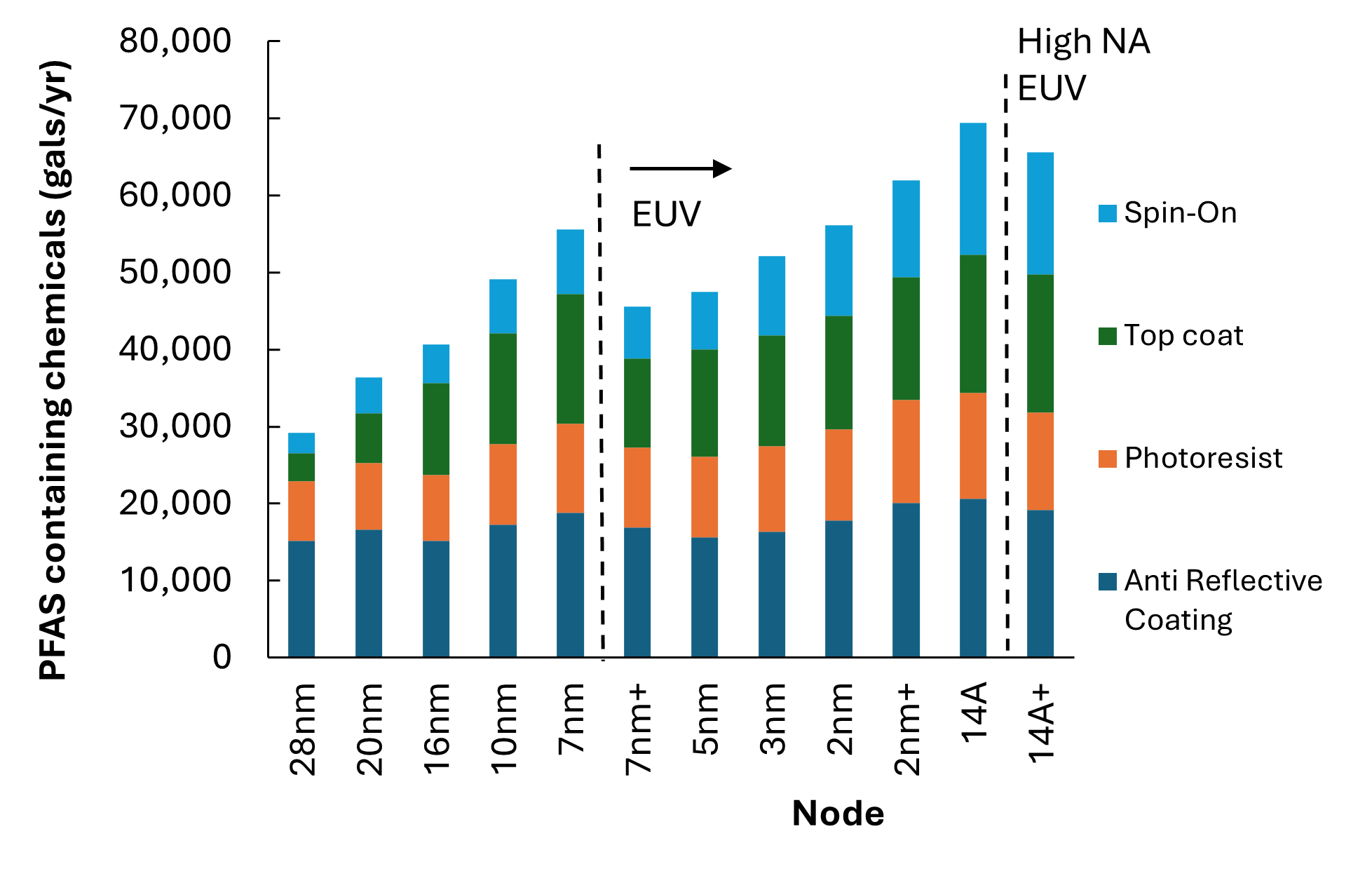
Figure 1: PFAS containing Chemicals by Technology Node. Source: TechInsights’ Semiconductor Manufacturing Carbon Model, Q4 2023 release.
The Environmental Challenge
Despite their utility, PFAS pose a significant environmental and health risk. Often called “forever chemicals,” PFAS exhibit remarkable persistence in the environment, resisting degradation over time. As a result, they accumulate in soil, water, and living organisms, posing a threat to ecosystems and human health.
In the semiconductor industry, PFAS contamination manifests through various channels. Wastewater discharges from manufacturing facilities can introduce PFAS into the environment, contaminating water sources and soil. The disposal of PFAS-containing materials complicates the situation further, perpetuating their presence in the ecosystem.
Regulatory and Industry Response
In response to growing concerns, regulatory bodies worldwide have begun to address the issue of PFAS contamination. Efforts to regulate the use and disposal of PFAS are underway, aiming to mitigate environmental pollution and safeguard public health. Initiatives such as the Stockholm Convention on Persistent Organic Pollutants seek to restrict the production and use of PFAS on a global scale, signaling a collective commitment to addressing this challenge. The Stockholm Convention has been successful in restricting the use of PFOS and PFOA, but there is still more work needed to limit PFAS through better understanding manufacturing processes and formulations of final products.
In early 2023, five countries in the European Union—Denmark, Germany, the Netherlands, Norway, and Sweden—submitted a proposal to the European Chemicals Agency (ECHA) asking for the restriction of PFAS. Discussions continue but this effort to contain PFAS usage only continues to gain attention—including work by the Environmental Protection Agency in the United States and some evolving efforts in Asia.
Within the semiconductor industry, stakeholders across the value chain are increasingly recognizing the importance of mitigating PFAS-related risks. Companies are exploring alternative materials and manufacturing processes to reduce reliance on PFAS and minimize environmental impact. Moreover, industry collaborations and research initiatives are underway to develop safer and more sustainable practices for semiconductor production.
The Future Starts Now
While daunting, participants across the semiconductor industry need to focus on ways to minimize PFAS contamination. By prioritizing environmental stewardship and adopting sustainable practices, stakeholders can mitigate the adverse effects of PFAS while ensuring the continued advancement of semiconductor technology.