Manufacturing Carbon Module
A Strategic Tool for Calculating Environmental Impact of Logic, Memory, and Power Technologies
TechInsights’ Manufacturing Carbon Module is the first of its kind to detail Scope 1, Scope 2, and Scope 3 carbon emissions by fab, location, wafer, and die. This is achieved by bringing together the equipment, processes, and manufacturing steps for Logic, DRAM, NAND, and select Gallium Nitride (GaN) and Silicon Carbide (SiC) processes into a single model for more than 400 fabs around the world.
The tool allows users to create their own unique analyses of carbon emissions with more than 2,500 customizable fields, including die yield, utilization, abatement, and electric carbon intensity based on their own assumptions and proprietary knowledge. Data available at user fingertips includes carbon emissions from electricity and on-site natural gas combustion, process chemical emissions and abatement, off-site emissions from the sourcing of raw materials, and water consumption. Renewable energy is also factored into calculations, where applicable, and itemized in the tool.
The Module enables users to compare fabs based on:
- Carbon emissions from purchased electricity
- On-site emissions from fossil fuel gas combustion, natural gas, and renewable energy
- Process chemical emissions and abatement efforts
- Off-site emissions from the sourcing of raw materials
- Water consumption by die and wafer
- Data available from 2015 through 2035 based on when fabs – past, current, future – come online
- More than 2,500 customizable fields allowing users to finetune assumptions

This module works in concert with TechInsights’ Packaging+ Carbon Module and Carbon Analyzer Module to leverage TechInsights' industry-leading expertise in reverse engineering and semiconductor manufacturing processes. Our proprietary databases combined with in-depth analysis and expertise provide the industry’s most comprehensive and reliable data available.
Manufacturing Carbon Dataset
Scope and Scale
The Manufacturing Carbon dataset is the most comprehensive emissions dataset ever assembled for semiconductor wafer fabrication. It covers:
- 400+ fabs worldwide
- 900+ processes
- 300mm leading-edge and legacy 200mm and 150mm wafer processes
- Coverage from 2015 through 2035
- Quarterly updates
What the Data Contains
The dataset is structured around three emission scopes, disaggregated at the fab, process, wafer, and die levels:

![]()
A Single Product for Cradle-to-Gate Sustainability Insights
EcoInsights is a comprehensive solution designed to help semiconductor companies drive significant environmental progress. With EcoInsights, users can quickly calculate the carbon footprint of over 30,000 integrated circuits (ICs) with cradle-to-gate transparency. It provides detailed insights into emissions from die manufacturing, packaging, and transportation. By identifying areas for improvement, companies can make data-driven decisions to reduce their environmental impact.
This powerful suite offers three integrated modules that deliver the data and tools needed for informed sustainability choices.

The Manufacturing Carbon Module is the first of its kind to detail Scope 1, Scope 2, and Scope 3 carbon emissions by fab, location, wafer, and die. It combines equipment, processes, and manufacturing steps for Logic, DRAM, NAND, as well as select Gallium Nitride (GaN) and Silicon Carbide (SiC) processes, into a single model for over 400 fabs globally.

The Packaging+ Carbon Module lets you calculate the carbon footprint of more than 30,000 ICs with standardized calculations based on packaging type, die size, and other factors. Get detailed analysis of Scope 1 and 2 from die manufacturing and Scope 2 and 3 emissions from packaging to track the impact of your entire supply chain.

The Carbon Analyzer Module offers a product-level overview of all integrated circuits in a device and their carbon footprints, down to the packaged IC level. It simplifies benchmarking and comparing semiconductor products and manufacturers on key sustainability metrics by detailing their environmental impact at both the component and function levels.

The EcoInsights System Carbon Module bridges the gap between product design and emissions accountability. Whether you're evaluating material choices, building sustainability into your roadmap, or meeting external reporting needs, this tool puts carbon visibility in the hands of decision-makers. Evaluate the full carbon footprint of electronic assemblies using the most accessible data available.


TechInsights’ Sustainability Tools Used to Drive Down Carbon Emissions in the Supply Chain
See how best-in-class fabless vendor was able to use the Manufacturing Carbon Module to deliver a full cradle-to-gate carbon emissions analysis of nearly 100 integrated circuits (ICs) to satisfy several customers’ reporting requirements.
Addressing Semiconductor Carbon Emissions: A Two-Part Challenge
As demands for semiconductor technology continue to increase, so do the impacts of the semiconductor industry on the environment. With the climate crisis intensifying, the semiconductor industry faces a two-part challenge:
- Design greener chips and the associated processes to reduce carbon emissions while simultaneously producing more powerful, and cost-effective semiconductors.
- Reduce carbon emissions from existing manufacturing facilities.
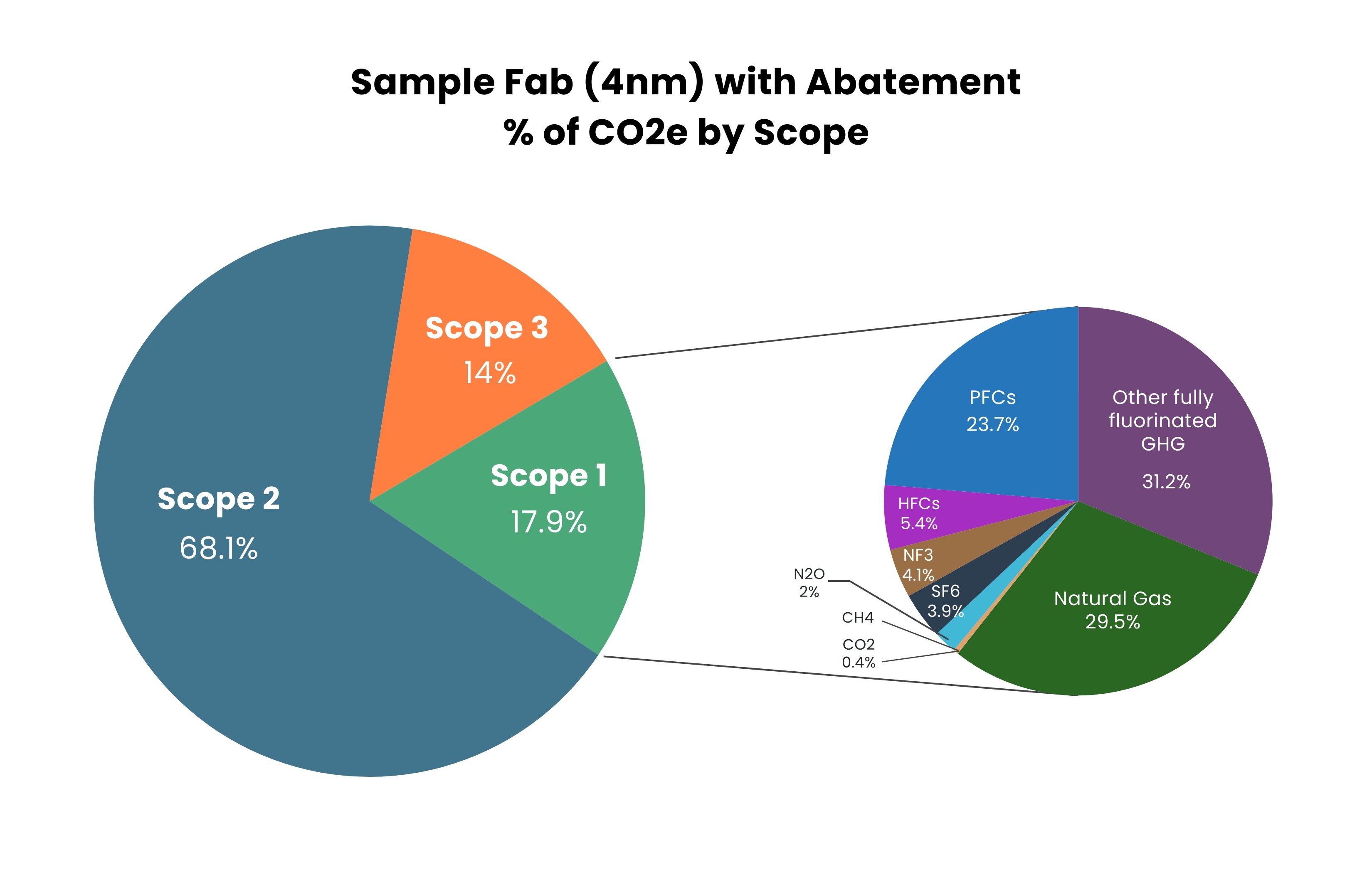
Examining Scope 1, 2, and 3 carbon emissions from manufacturing a die, with breakout for Scope 1 emissions. Source: TechInsights’ Manufacturing Carbon Module, 2024.
Manufacturing Carbon Module Overview
The Manufacturing Carbon Module calculates Scope 1, 2, and 3 carbon emissions from integrated circuit manufacturing of chips measuring 3,000nm to 10A, including logic and memory (NAND and DRAM), and known fabs coming online in the next several years. Select silicon carbide (SiC) and gallium nitride (GaN) processes, and associated fabs, are also included. Scope 1 emissions are further broken down by natural gas and individual process gases. Scope 3 emissions cover more than 240 raw materials and chemicals. The Module provides carbon emissions and water consumption from 2015 to 2035, allowing users to compare historical results to current and future scenarios.
The Module makes it possible to review and compare electricity, carbon emissions, and process gases for each piece of equipment used. Equipment categories include atomic layer deposition (ALD), backgrind, chemical vapor deposition (CVP), chemical mechanical polishing (CMP), dry etch, implant, inspection, lithography, metrology, plating, physical vapor deposition (PVD), spin-on, thermal and wet cleans.
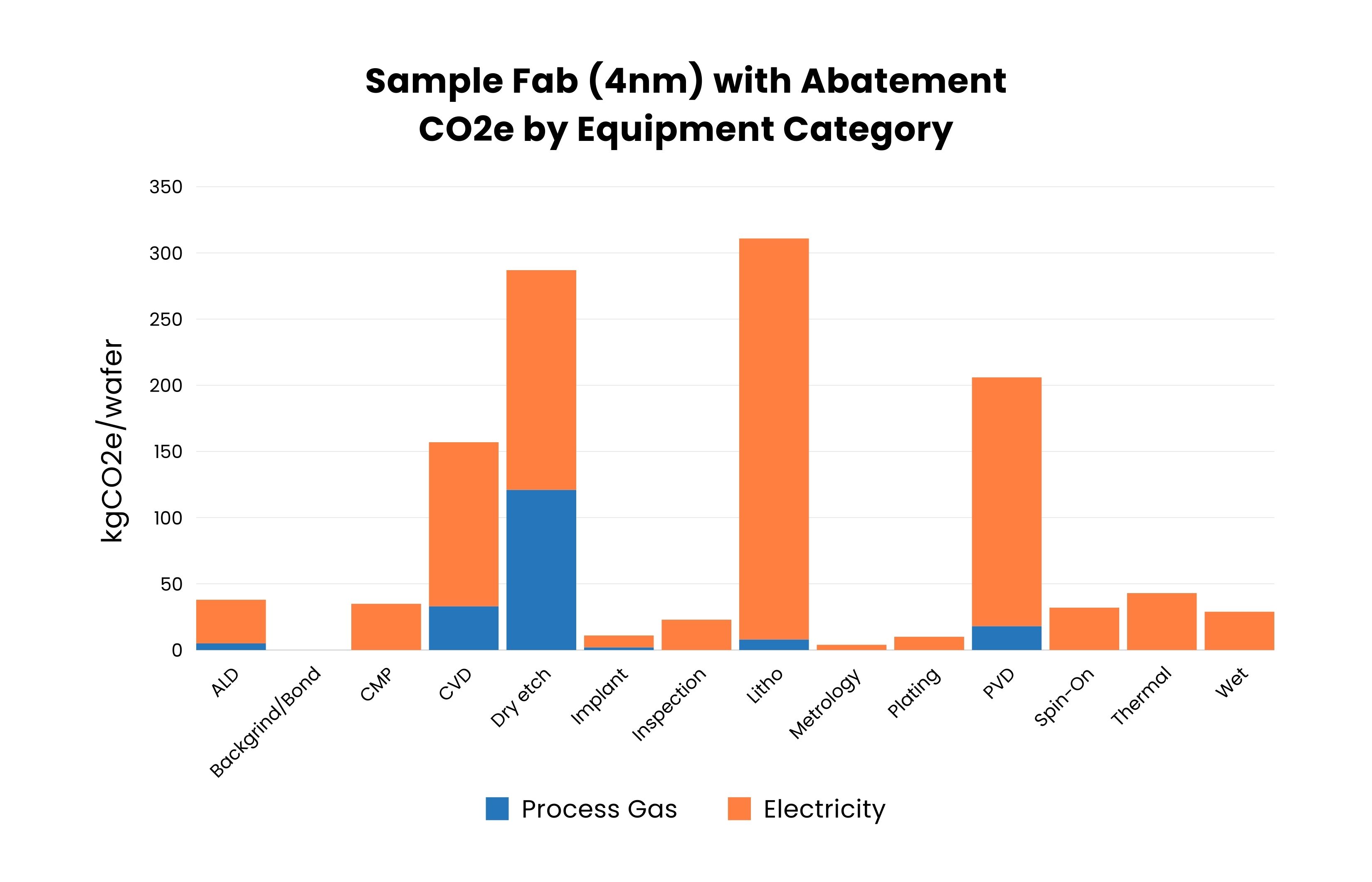
Breakdown of Carbon Emissions by Equipment Type from process gas and electricity. Source: TechInsights’ Manufacturing Carbon Module, 2024.
Insights in the Manufacturing Carbon Module include:
- CO2e emissions and water consumption by node at a fab, die, and wafer level
- Emissions at the equipment and process level
- Future emerging technology and electricity mix impact on carbon emissions and water consumption
- Detailed emissions and water consumption for customized fabs as well as fabs currently under construction or planned.
Get answers to key questions about semiconductor carbon impacts and how the industry is working to decrease emissions.
Supporting Your Business in Its Sustainability Reporting
Covering more than 400 fabs, the TechInsights Manufacturing Carbon Module is a vital sustainability tool providing the detailed modeling and benchmarking that supports many areas of the semiconductor value chain, including:
- Capital Equipment vendors see value with the Module providing a critical business development tool to compare and benchmark tools versus the competition, while also being able to understand the abatement levers that help reduce emissions.
- Foundries can use the editable fields for scenario analysis; and facilitates understanding of abatement on carbon emissions and electricity consumption, as well as run competitor comparisons.
- Fabless Vendors gain a fact-based understanding of die size on carbon emissions, electricity consumption and water use. The Module also enables scenario analysis.
- Integrated Device Manufacturers (IDMs) use the tool to support key design decisions and evaluate investment decisions for new equipment and tools.
- Product Manufacturers use the Manufacturing Carbon Module provides key inputs into cradle-to-grave analysis and reporting.
- Automotive Manufacturers use the Manufacturing Carbon Module to understand the carbon emissions associated with electronic components being used in vehicles, in conjunction with costing information from TechInsights’ Strategic Cost and Price Model.

NVIDIA HGX B300 Benchmarking for AI Infrastructure
Access TechInsights' NVIDIA HGX B300 benchmarking analysis to evaluate AI infrastructure performance, power, thermal behavior, and multi-GPU scaling.

Apple M5 Pro Package Analysis: TSMC's SoIC-X F2F Hybrid Bonding in Consumer Computing
TechInsights analyzes the Apple M5 Pro APL1X15 package, revealing TSMC SoIC-X F2F hybrid bonding, CPU and GPU chiplets, silicon interposer routing, and verified die costs.

Why the AI Memory Shortage Could Keep DRAM and NAND Prices High for Years
AI-driven demand is creating the biggest memory shortage in history. Discover why DRAM and NAND prices are expected to remain elevated through the rest of the decade.
![]()
The Authoritative Information Platform to the Semiconductor Industry.

