Contributing Authors: Ray Fontaine
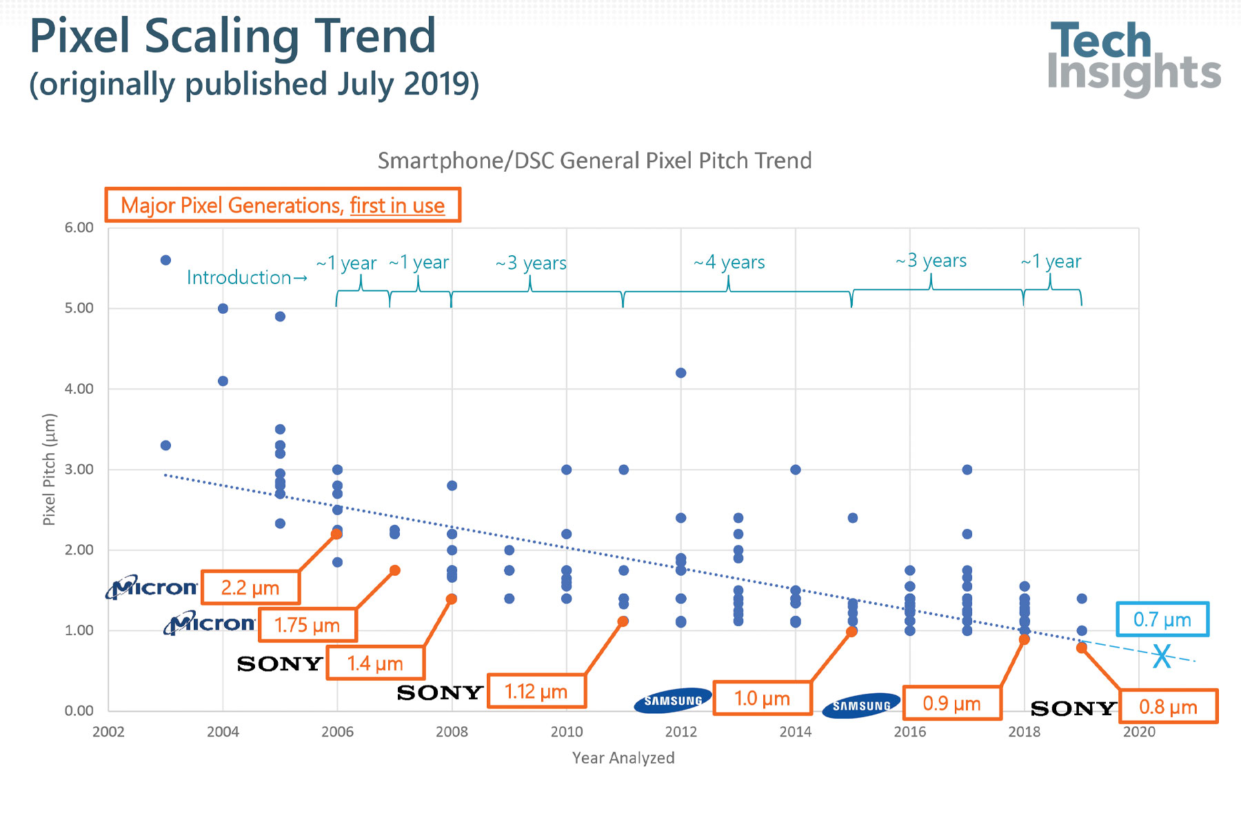
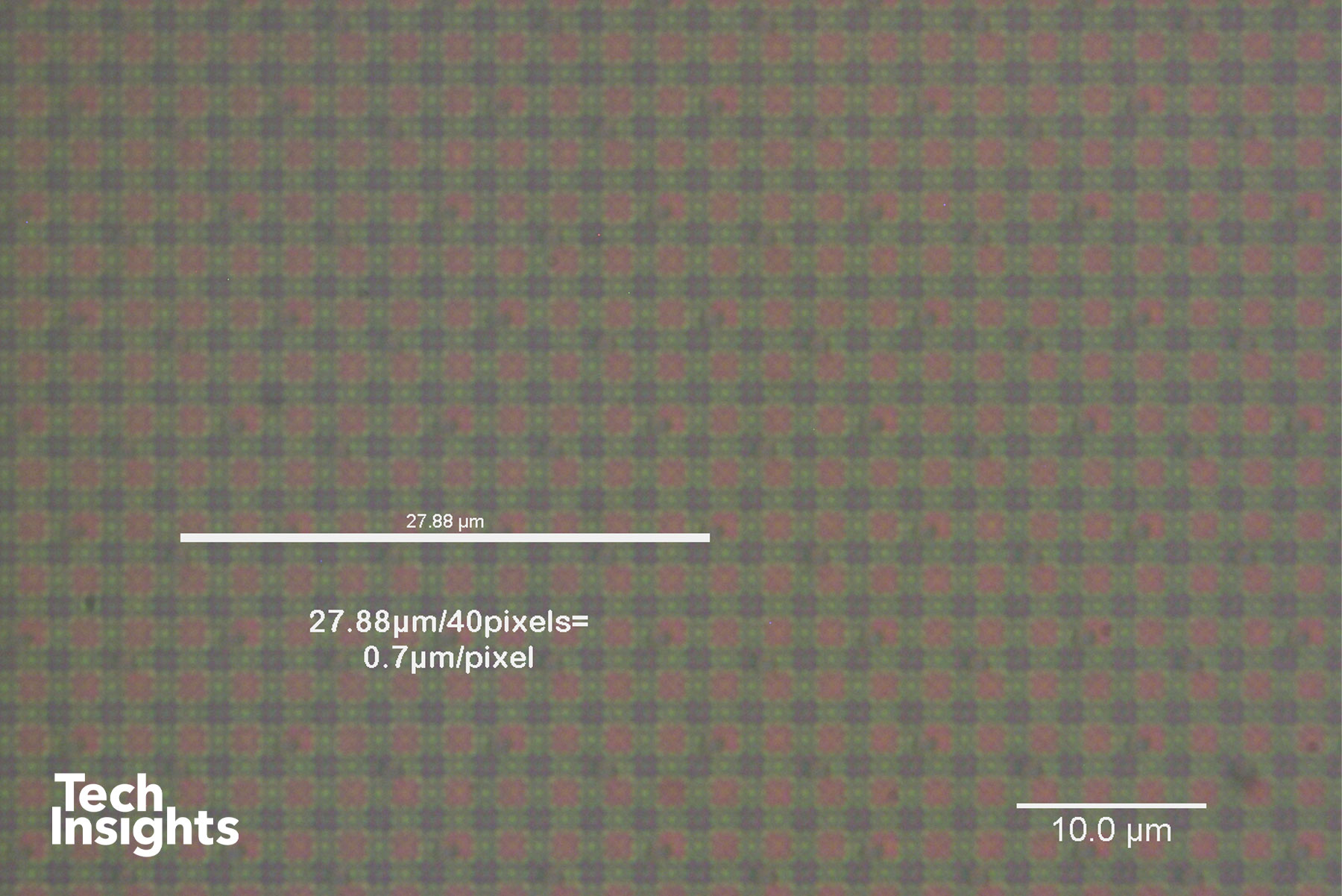
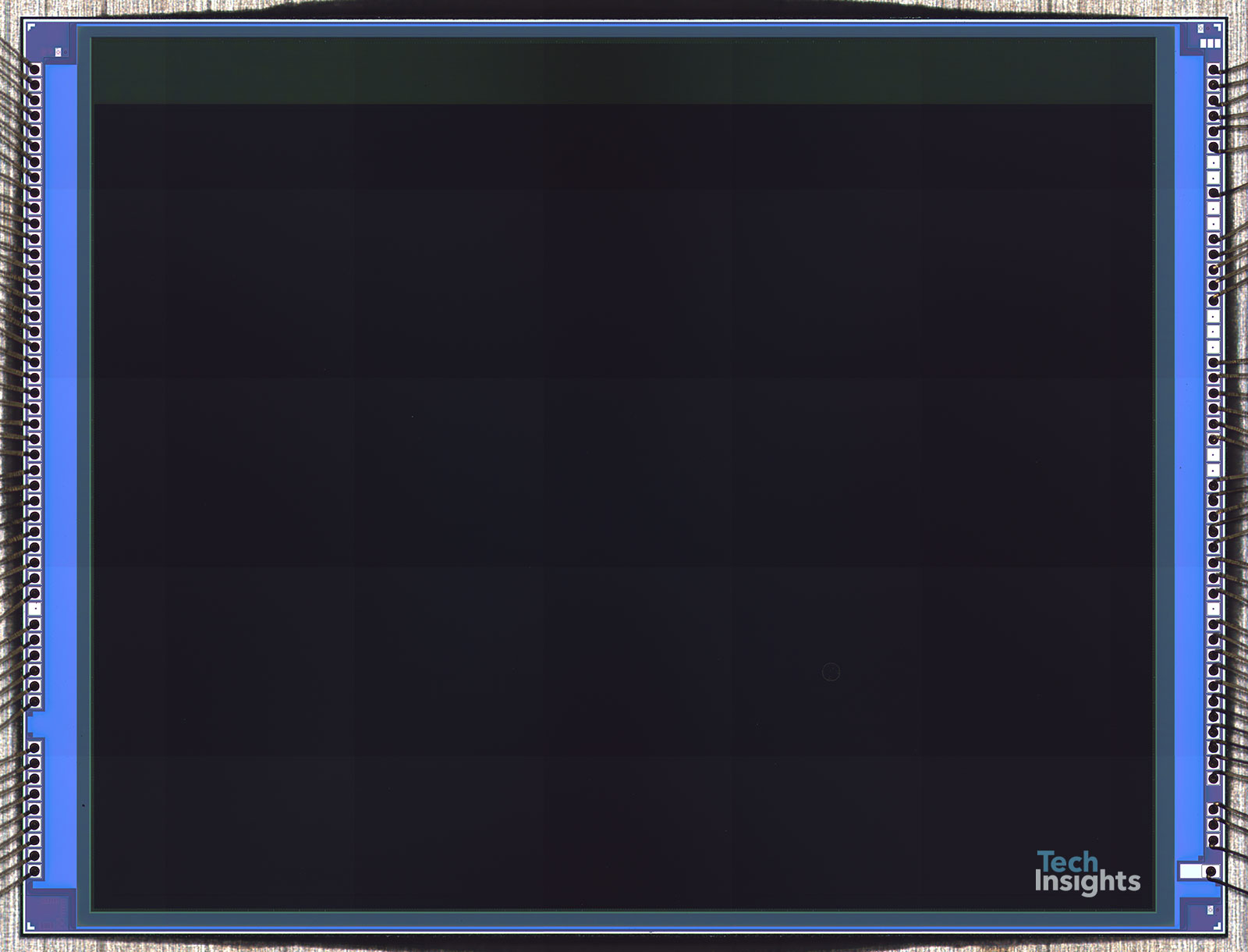
Congratulations to the Samsung team for not only delivering a well spec’d camera system, but also for being first to market with 0.7 µm generation pixels! The GH1 stacked imager, announced in September 2019, is in use in the S20 Ultra 5Gs front-facing camera. Referring to our discussion of small-pixel market availability from July 2019, the trendline on our data shows the 0.7 µm pixels in S20 Ultra 5G have arrived right on schedule. At the time we had expected it would take another few quarters to march deeper into sub-micron pixel territory, so we are happy the trendline got it right. It is not a trivial accomplishment and we are eager to dig into the GH1s enabling technology elements.
The GH1, which uses ISOCELL Plus technology, has a reported resolution of 7968 x 5840 (43.7 MP). The die we are analyzing is 5.13 mm x 6.51 mm (33.4 mm2) with an active pixel array size of 3.89 mm high by 5.63 mm wide (6.84 mm diagonal). The Tetracell color filter array is in use and manipulating the contrast on our optical images we can see an artifact of the Super-PD phase detection autofocus (PDAF) pixel pattern. We have documented Samsung using masked and 2x1 on-chip lens (OCL) PDAF on different 0.8 µm generation sensors. Here at the 0.7 µm generation we expect only 2x1 OCL PDAF will be used, as on the GH1.
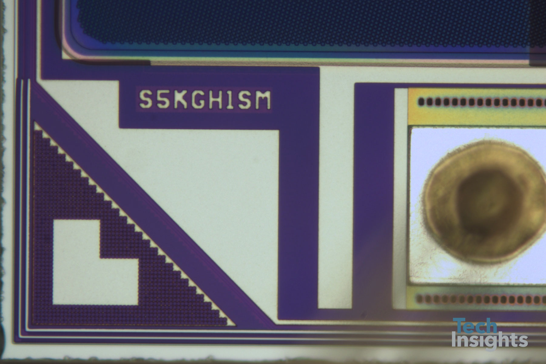
One other topic to mention on this world’s first 0.7 µm pixel sensor is the stacked chip interconnect strategy. The through silicon via (TSV) arrays visible in our die photograph show us immediately that Samsung has not yet adopted a Cu-Cu direct bond interconnect strategy as we have observed in Sony and TSMC fabricated imagers.
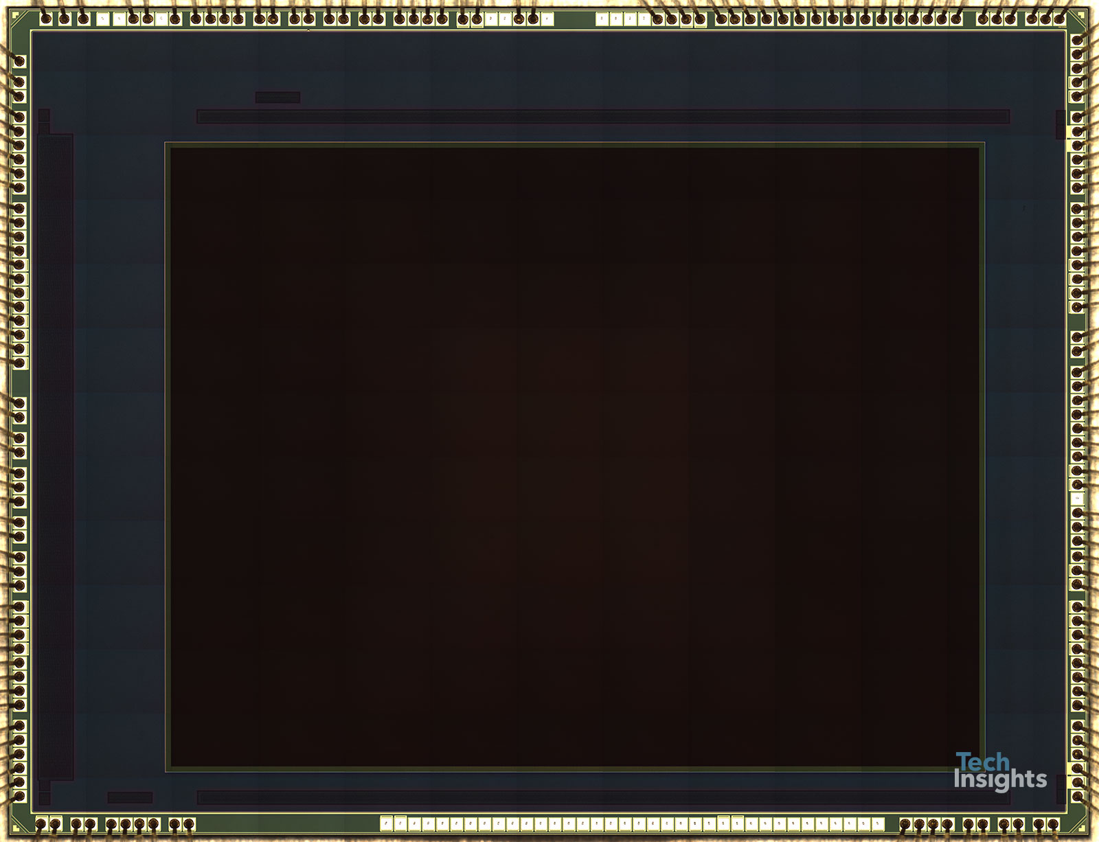
The S20 Ultra 5G’s 12 MP ultra-wide angle rear-facing camera features the Samsung S5K2L3SX imager, a recycled triple-stacked imager first in use in 2018 in Galaxy S9+. The S5K2L3SX features 1.4 µm generation pixels, dual PD PDAF and a Bayer RGB CFA. The die size is 5.88 mm x 7.68 mm (45.2 mm2).
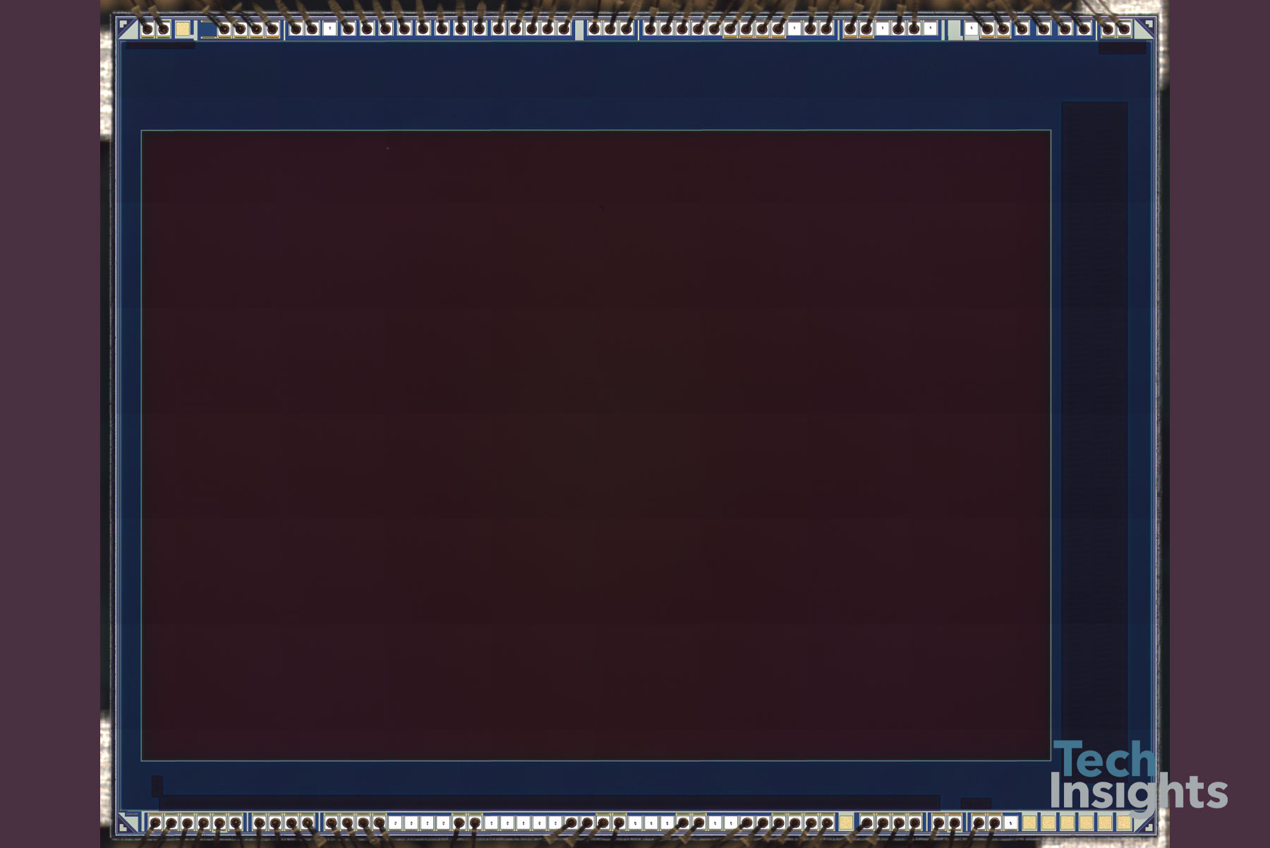
S5K2L3SX Die Photograph
![]()
S5K2L3SX CFA
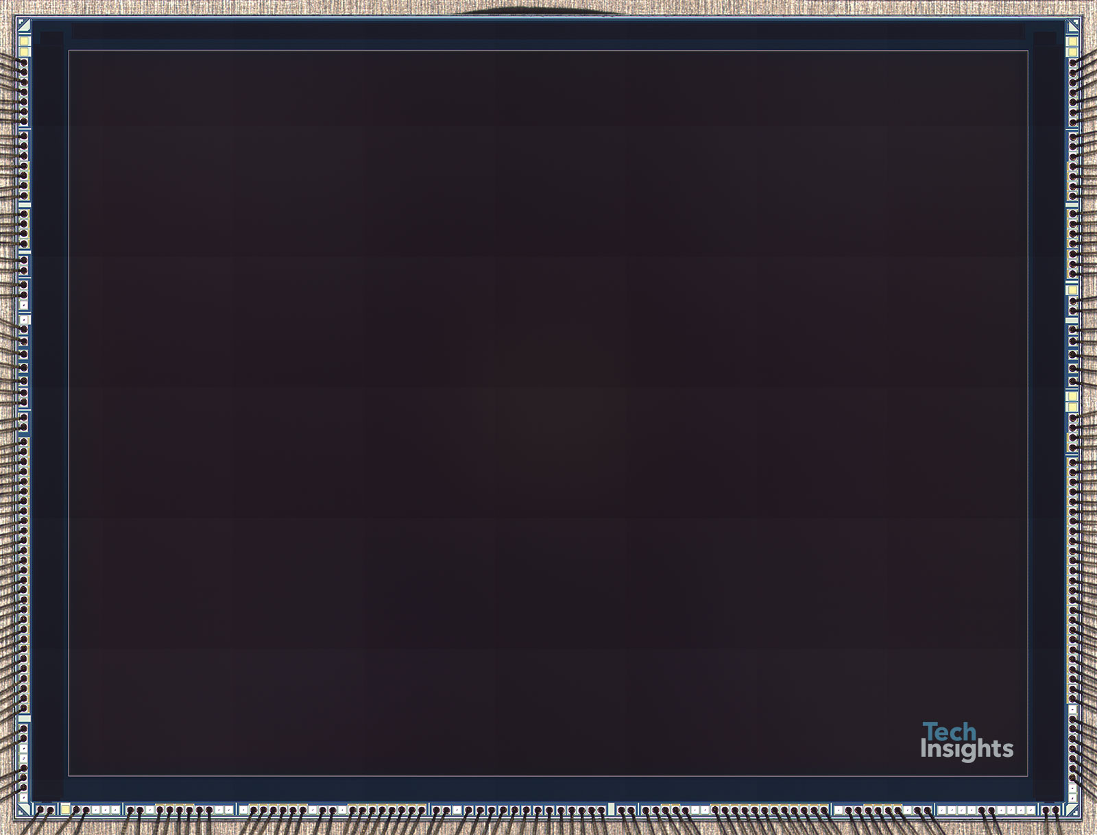
The S20 Ultra 5G’s 108 MP wide-angle rear-facing camera is new to Samsung’s Galaxy smartphones and is the centerpiece of this multi-camera system. We have reported on the 108 MP HMX, in use in the Xiaomi Mi CC9 Pro from November 2019, but here in the Ultra’s system a new variant, the HM1 is used. The HM1 features the first implementation of Samsung’s Nonacell 3x3 pixel/color filter architecture. We have also had a first look at the HM1s stacked image signal processor (ISP) die and it is clear there is a lot more logic and memory in use, as compared to the sparsely populated HMX ISP.
The HM1 die size is 8.17 mm x 10.82 mm (88.4 mm2). The pixel pitch is 0.8 µm while the color filter pitch is 2.4 µm. Our preliminary optical images reveal a new dual 2x1 on-chip lens (OCL) phase detection autofocus (PDAF) layout spanning select blue/green and red/green pixel pairs.
HM1 Die Photograph
![]()
HM1 Nonacell CFA and Dual 2x1 OCL PDAF
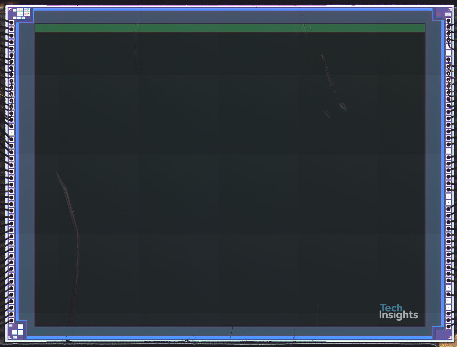
A Sony IMX586 is used in Galaxy S20 Ultra’s 48 MP telephoto camera. It was Sony’s first 0.8 µm generation imager and it is a chip we first found in use in early 2019. The IMX586 is 5.62 mm x 7.47 mm (42.0 mm2) and features a Quad Bayer CFA and 2x1 OCL PDAF.
Sony IMX586 Die Photograph
![]()
Sony IMX586 CFA and 2x1 OCL PDAF
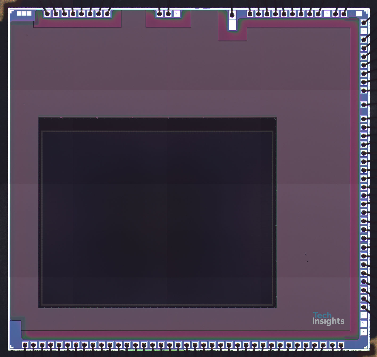
The indirect time-of-flight (i-ToF) sensor appears to be a Sony IMX516. We had seen speculation of a new part number (IMX518) in use for S20 Ultra 5G, but at this moment we are unable to distinguish any differences in the die photos between this sensor and our existing IMX516 analysis. The IMX516 features a 640 x 480 resolution, 5 µm pixel pitch and 5.11 mm x 4.85 mm (24.8 mm2) die size.
Sony IMX516 i-ToF Die Photograph
That completes our overview of the Galaxy S20 Ultra 5G’s camera system. We look forward to DXOMARK’s performance review to see how this new camera system ranks against the current #1 ranked (as of March 2) Xiaomi Mi 10 Pro.
Galaxy S20 Ultra 5G Camera Chip Overview
| Orientation | Camera | IC Configuration | Image Sensor Si Vendor |
Die Size (mm2) | Resolution (MP) | Pixel Pitch (µm) | CFA | PDAF |
|---|---|---|---|---|---|---|---|---|
| Rear-Facing | Ultra-Wide | Back-illuminated, stacked (3-die) | Samsung | 45.2 mm2 | 12 | 1.4 | Bayer RGB | Dual PD |
| Rear-Facing | Wide-angle | Back-illuminated, stacked (2-die) | Samsung | 88.4 mm2 | 108 | 0.8 | Nonacell | Dual 2x1 OCL |
| Rear-Facing | Telephoto | Back-illuminated, stacked (2-die) | Sony | 42.0 mm2 | 48 | 0.8 | Quad Bayer | 2x1 OCL |
| Rear-Facing | DepthVision | Back-illuminated, monolithic | Sony | 24.8 mm2 | 640 x 480 | 5.0 | Not in use | Not in use |
| Front-Facing | Selfie | Back-illuminated, stacked (2-die) | Samsung | 33.4 mm2 | 40 | 0.7 | Tetracell | Not in use |
We have several projects in progress on the S20 5G, S20 5G + and S20 Ultra 5Gs phones and imagers. Within our image sensor subscription vertical we are studying the most innovative imagers and stacked ISPs. This includes our SEM-based Device Essentials (DEF) analyses and our complete process analysis featuring TEM, TEM-EDS, SIMS, SCM, etc. in our Device Essentials Plus (DEP) format. From a design aspect we are publishing high-resolution poly die photographs of select stacked ISPs and are working on circuit analysis reports (CAR) of the HM1 and the Sony IMX555 from Galaxy S20 5G and S20+ 5G.
Since we have mentioned here in this S20 Ultra 5G teardown blog, it is worth sharing some preliminary findings of the IMX555 from S20/S20+ 5G. The IMX555 has a die size of 6.45 mm x 8.46 mm (54.6 mm2) and a 1.8 µm pixel pitch.
Sony IMX555 (from S20/S20+ 5G) Die Photograph
![]()
Sony IMX555 (from S20/S20+ 5G) CFA
Image Sensor Subscription Content (Galaxy S20+ 5G, S20 Ultra 5G Cameras)
| Vendor | Part Number | Process Report Codes | Design Report Codes |
|---|---|---|---|
| Samsung | S5KGH1 | DEF-2002-801, DEP-2002-801 | |
| Sony | IMX555 | DEF-2002-803 | CAR-2002-808 |
| Samsung | S5KHM1 | DEF-2002-802 | CAR-2002-807 |
Find content like this and more in the TechInsights Platform. Sign-up for free today.


