4-Part Blog Series: The state of the art of smartphone imagers
Part 2: Pixel Scaling and Scaling Enablers
Posted: July 16, 2019
Contributing Author: Ray Fontaine
Content adapted from TechInsights’ paper for the International Image Sensors Workshop (IISW) 2019
Blog outline of the talk was structured in four parts:
(1) chip-stacking and chip-to-chip interconnect,
(2) pixel scaling and scaling enablers,
(3) active Si thickness and deep trench isolation (DTI) structures, and
(4) non-Bayer color filter arrays, and phase detection autofocus (PDAF).
There is no Moore’s Law equivalent for pixel development, however there have been natural pixel generations, a metric derived from optical system and array resolution requirements. Figure 1 illustrates the first documented use of new pixel generations by year
In reviewing TechInsights’ library of analysis back to the 2.2 µm generation, Micron Imaging led pixel generations from that point through to the 1.75 µm generation. After that, Sony famously maneuvered to take the lead in CMOS image sensor technology and was first to have its 1.4 µm and 1.12 µm pixels in downstream product. Then came Samsung, out first in the 1.0 µm generation.
It’s worth pausing here and recalling an informal audience poll facilitated by Lindsay Grant at Image Sensors Europe 2010: Lindsay asked the audience how many believed sub-micron pixels would ever be realized in mass produced imagers. As I recall, less than 1/3 of the audience believed it would be possible.
And here we are in 2019 with 0.8 µm pixels in wide use in recent smartphones! Samsung was first out with 0.9 µm pixels in 2018 - Sony is flagged as first in use, but it generally could be considered a tie between Sony and Samsung, with host phones released months apart.
At TechInsights, as technology analysts we are often asked to predict: what’s next? So, what about scaling down below 0.8 µm? Of course, 0.7 µm and smaller pixels are being developed mostly in secrecy, including for non-obvious use cases. For now, we will stick with our trend analysis and suggest that if a 0.7 µm generation is going to happen, it may be ready for the back end of 2020 or in 2021.
The realities of the visible light spectrum are not going to change, so scaling possibilities are not infinite. One final comment on this plot is the annotation marking the approximate time between pixel generation introductions, a topic expanded on in the next figure.
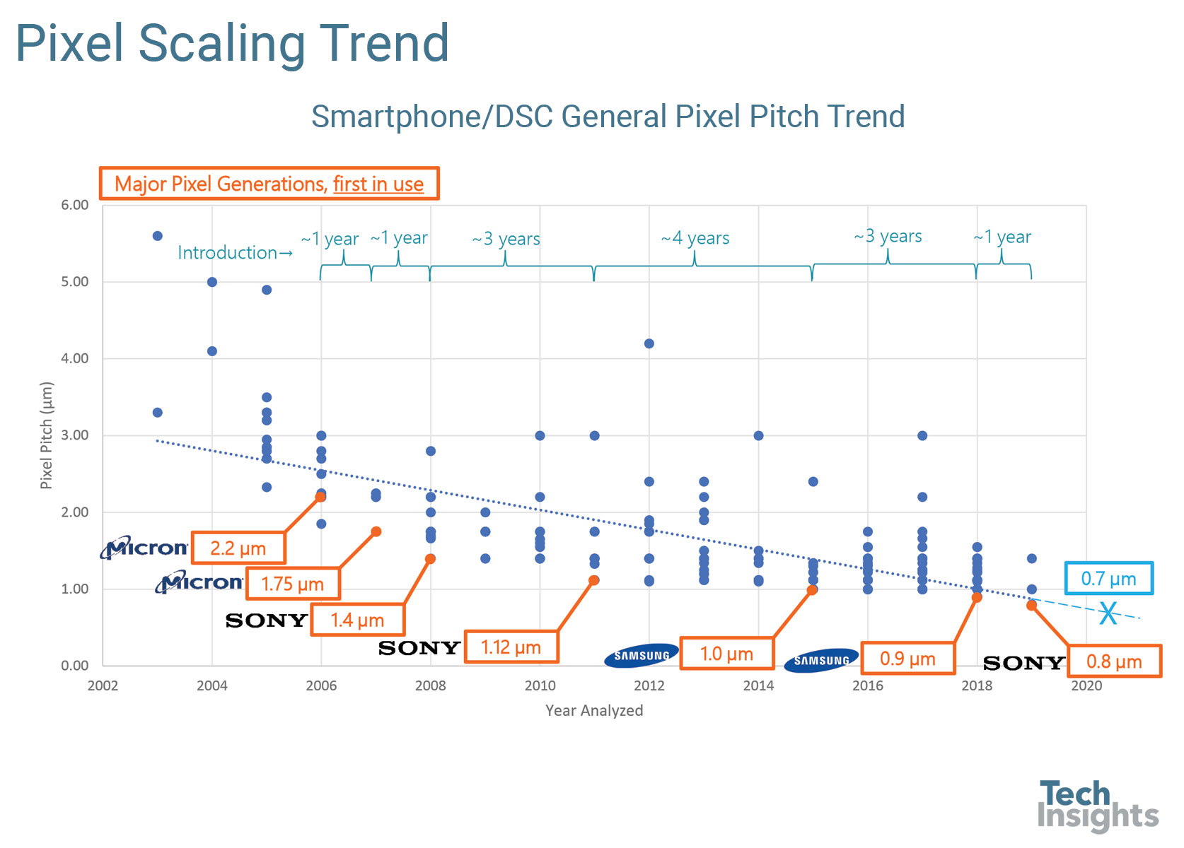
Figure 1: Small-Pixel Selected Small Pixel Scaling Enablers
The State-of-the-Art of Smartphone Imagers
Download our paper and slides from TechInsights' presentation at IISW 2019.
Selected pixel scaling enablers are shown on the same data set in Figure 2 illustrating the introduction of pixel generations. The intent is to show the first known use of major technology elements, starting with the use of light pipes as a strategy to extend the life of front-illuminated pixels, or more accurately a means to defer investment in back-illuminated technology development.
BI CMOS pixels were realized by Sony and OmniVision in 2009 and the substantial development effort coincided with a slowing of new pixel introduction. Soon after BI pixels were developed, high-k passivation films were introduced. It is worth reiterating these markers are all first use; each technology element continues to evolve.
BI sensor configuration was a paradigm shift; however, its benefits were not fully realized until the introduction of deep trench isolation (DTI) schemes. STMicroelectronics successfully launched imager products with DTI, however Apple’s launch of iPhone resulted in eventual obliteration of Nokia and Blackberry’s mobile phone market share. STMicroelectronics got caught in the supply chain disruption and its development efforts for small-pixel mobile were negatively impacted.
While for a time it seemed STMicroelectronics might become small-pixel leaders, it was instead Sony and Samsung that pushed their respective DTI solutions into wide use. It’s a common misconception that Samsung was first to use vertical transfer gates (VTG) in an imager with its ISOCELL imagers. We found Sony to be using VTG in 2013, albeit for a single generation (and only reintroduced in its 2018 IEDM paper on BI global shutter). Samsung introduced full front-DTI (F-DTI) in 2013 and buried (embedded) color filter arrays (CFA) in 2015.
The absence of major callouts in 2016 and onward do not correlate to inactivity. The innovation we have been documenting in leading edge parts of recent years could be described as incremental, although it is a subjective assessment. In recent times we have been uncovering many interesting optimizations of the described technology elements, and the literature, including IISW 2019 papers, road map some clever next steps. In summary, it is our belief that development of DTI and associated passivation schemes was the main contributor to delayed pixel introduction of 1.12 µm down to 0.9 µm pixels.
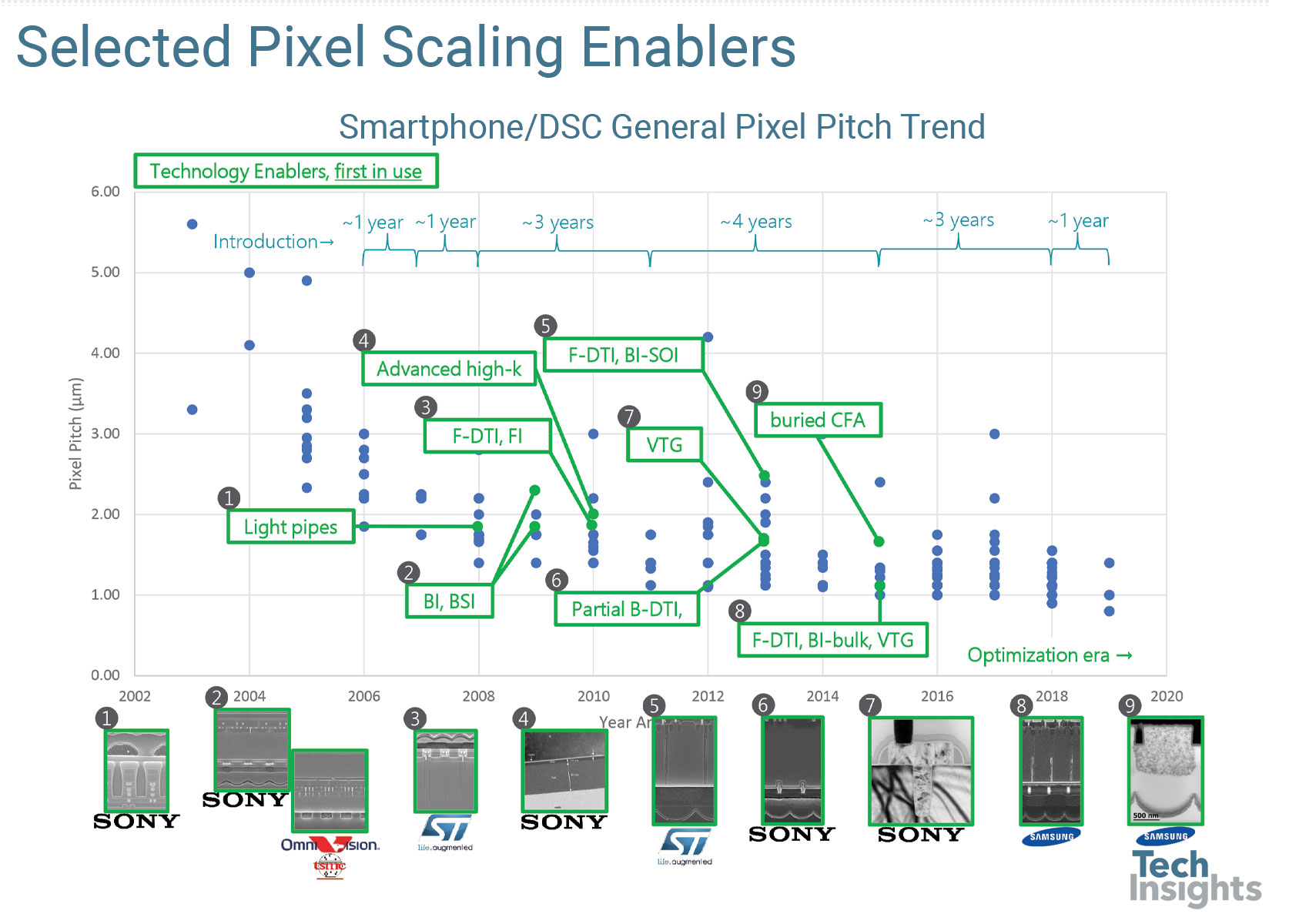
Figure 2: Selected Small Pixel Scaling Enablers
In the next post we’ll discuss the trend in active Si thickness for back-illuminated smartphone imagers and the trend in deep trench isolation (DTI) structures.
The Trusted Technical Intelligence Provider
TechInsights has been at the forefront of image sensor competitive technical intelligence since 2006, and have always been the first to report on key technology elements. All Top 10 image sensor design companies are our subscribers, and all Top 3 image sensor foundries are our subscribers.


