The "Hidden" Phase: Why Your Carbon Strategy Needs to Shift to the Fab
For years, the semiconductor industry has been locked in a race for operational efficiency. We have pushed performance-per-watt and software optimizations to their limits, assuming that energy-efficient devices were inherently "green." However, recent discussions at the Chiptainability Online Seminar Series 2026—in partnership with Nokia and the University of Würzburg—highlighted a critical oversight: we have been largely ignoring the carbon footprint established before a device ever leaves the factory.
Moving Beyond Runtime Energy
The central issue is a reliance on industry-average proxies for manufacturing emissions. This is a flawed approach because semiconductor fabrication is influenced by highly volatile factors: specific grid mixes, abatement system efficiency, and process-specific gas usage.
When we rely on approximations, we miss the "manufacturing reality." Two devices with identical performance can carry vastly different carbon burdens, and without fab-specific intelligence, these differences remain invisible to decision-makers.
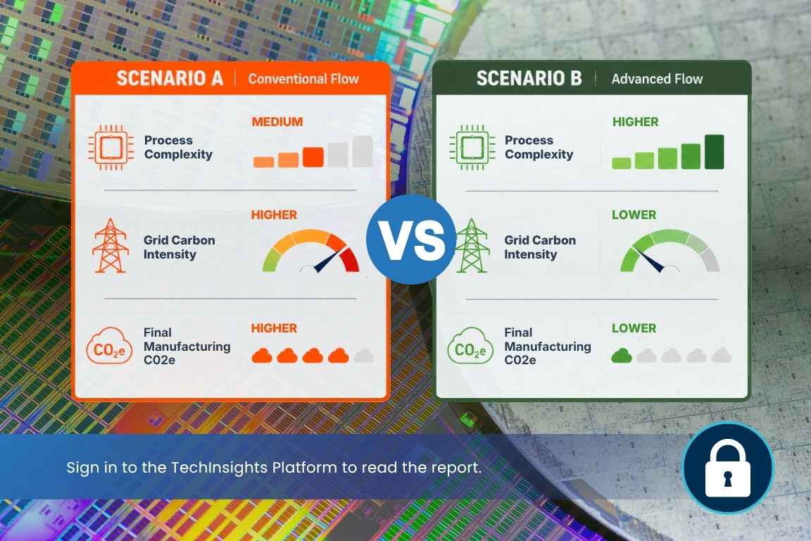
Figure 1 – The “greener” option depends on process design, fab location, electricity mix, and yield conditions. (Source: TechInsights)
The Complexity Trap
As we advance toward 2nm logic and beyond, the carbon intensity of manufacturing is not shrinking—it is expanding. The shift toward Extreme Ultraviolet (EUV) lithography and multi-patterning means that new nodes can be 2.5 to 3.5 times more carbon-intensive than their 90nm predecessors.
This creates a paradox where pushing for "better" performance can inadvertently increase the total lifecycle carbon debt. The takeaway for engineers is clear: technological progress must be balanced against the rising complexity of fabrication.
Adopting "Decision-Grade" Metrics
To address this, we advocate for "decision-grade" Product Carbon Footprints (PCFs). These are not just estimates; they are rigorous data sets that require:
- Total Traceability: Connecting outcomes to specific processes, tools, and fabs.
- Boundary Transparency: Clearly defining the functional units used in calculations.
- Uncertainty Quantification: Accounting for yield rates and grid variations.
- Assurance Readiness: Ensuring documentation is standardized for independent verification.
When sustainability becomes a quantifiable engineering parameter, designers can perform scenario-based analysis—comparing, for instance, front-side versus backside power delivery with full awareness of the carbon tradeoffs involved. Tools like the TechInsights Manufacturing Carbon Module allow teams to treat carbon as a design variable rather than a retrospective reporting metric.


