Samsung K4VOF165ZC D1b 12 Gb GDDR7 DRAM Memory Floorplan Analysis
What does Samsung's latest D1b-generation GDDR7 DRAM reveal about the future of AI, HPC, and GPU memory technology?
TechInsights has completed a comprehensive Memory Floorplan Analysis (MFR) of the Samsung K4VOF165ZC 12 Gb GDDR7 DRAM die found inside the Samsung K4VCF325ZC-SC28 package. This report provides detailed insight into Samsung's D1b DRAM process technology, memory architecture, floorplan organization, critical dimensions, process integration, and manufacturing cost.
The K4VCF325ZC-SC28 is a high-density 3 GB GDDR7 SDRAM designed for AI accelerators, high-performance computing systems, and next-generation graphics processors. Featuring a dual-die architecture and PAM3 signaling, the device delivers significantly higher bandwidth than previous GDDR generations while leveraging Samsung's fifth-generation 10 nm-class DRAM technology and EUV lithography.
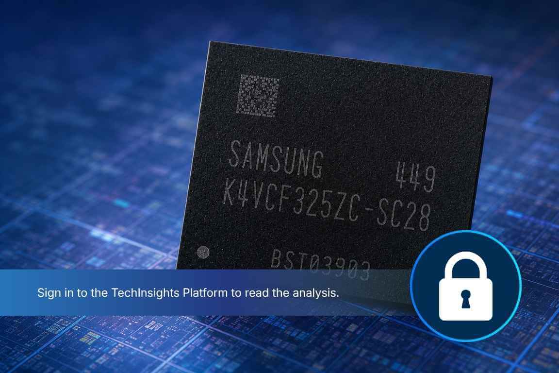
Figure 1 – Gain exclusive insight into Samsung's D1b 12 Gb GDDR7 memory technology, including floorplan architecture, process integration, critical dimensions, manufacturing cost analysis, and high-resolution CircuitVision imagery. (Source: TechInsights)
TechInsights' analysis reveals a highly optimized floorplan consisting of two memory regions separated by a central peripheral circuit strip containing I/O, command and control logic, eFLASH, and global data path circuitry. The report also examines memory array organization, peripheral circuitry, die utilization, and process technology scaling that enable Samsung's latest GDDR7 implementation.
The report includes:
- Package photographs, X-rays, die markings, and die photography
- Functional block identification and floorplan analysis
- Memory array and peripheral circuit architecture
- SEM cross-sectional and plan-view process analysis
- Critical dimension measurements
- Die utilization and block size analysis
- Manufacturing cost analysis
- High-resolution top metal and gate-level die images delivered in CircuitVision
This analysis is valuable for memory manufacturers, semiconductor designers, equipment and materials suppliers, competitive intelligence teams, and organizations developing AI infrastructure, graphics processors, and advanced computing platforms.


