AlixLabs and VDL ETG Projects Announce MoU for APS Patterning Technology Industrialization
2 Min Read April 10, 2026
AlixLabs and VDL ETG partner to industrialize APS™ patterning, moving the technology from R&D to production‑ready tools for advanced fabs.
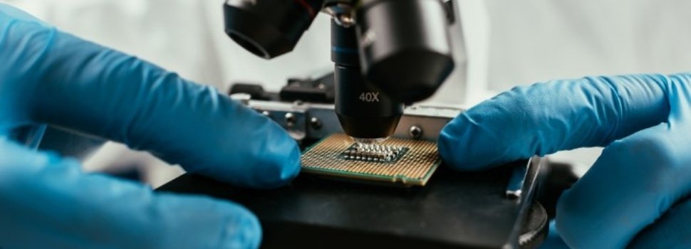
AlixLabs and VDL ETG Projects signed an MoU to industrialize APS™ (Atomic Pitch Splitting) patterning technology, aiming to scale production of advanced semiconductor equipment for next-generation fabrication. APS™, based on atomic layer etching, offers a cost- and energy-efficient alternative to complex EUV and multi-patterning processes, enabling precise feature scaling for logic and memory chips. Under the partnership, VDL will support system integration and manufacturing to transition APS™ from R&D to production-ready tools, accelerating adoption in semiconductor fabs and improving production efficiency.
This summary outlines the analysis* found on the TechInsights' Platform.
*Some analyses may only be available with a paid subscription.


