Industry-leading DDR5 Technology: Micron vs. Samsung vs. SK Hynix
We have just entered into the era of DDR5 memory. All the major DRAM players such as Micron, Samsung, and SK Hynix have started to release their first DDR5 memory products (modules) since last year. Further, demand for DDR5 products is significantly and surely exceeding supply nowadays. DDR5, the new standard in DRAM, is aimed at the demands of computing, high bandwidth, artificial intelligence (AI), machine learning (ML), and data analytics.

Jeongdong Choe
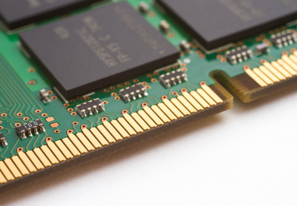
DDR5 memory product.
DDR4 data rates generally operate in a range from 1,600 MHz to 3200 MHz, while DDR5 improves on DDR4 with both data and clock rates, doubling the performance at up to or more than 7,200 megabits per second (Mbps). DDR5 lowers the operating voltage to 1.1V. Many new and advanced features have been added and modified including the increased prefetch from 8 to 16, more banks and bank groups to increase bus efficiency, new write pattern and refresh modes, decision feedback equalizer (DFE), and PDA as well. On-die ECC is also added to strengthen the on-chip RAS and reduce the burden on the controller. It is surely one step closer to unlocking the value in future data-centric applications.
Subscribe to TechInsights Blogs
Join our list to get the latest blog posts directly in your email.
The first DDR5 products hit the market with UDIMMs, running at 4,800 MT/s (or 5,600 MT/s). This is a 33% increase in data rate over top-end 3,200 MT/s DDR4 DIMMs in current high-performance servers. For reference, Everspin 1 Gb pMTJ STT-MRAM stand-alone DDR4 chips operate at 1,333 MT/s with 15 ns CL and 135 ns tRCD. Recently released GDDR6 devices are running at 16,000 MT/s, LPDDR5 at 6,400 MT/s, and 3,600 MT/s for HBM2E, the latest version of Nvidia’s flagship data center GPU, the A100 with 80 GB (Figure 1).
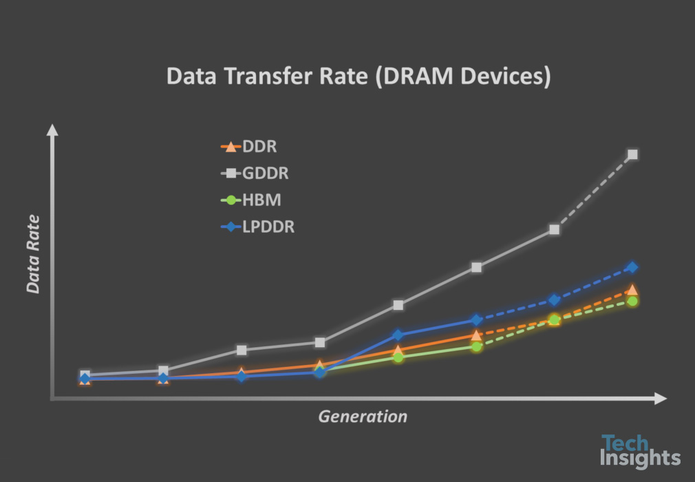
Figure 1. DRAM data rate trends for DDR, GDDR, HBM, and LPDDR.
JEDEC recently updated the DDR5 SDRAM standard (JESD79-5A) including the demand requirements being driven by intensive cloud and enterprise data center applications, providing developers with twice the performance and much-improved power efficiency. For higher density and higher performance, DDR5 is expected to adopt the most advanced DRAM cell technology nodes such as D1z or D1a (D1α) generation which is the 3rd or 4th generation of the 10-nm class DRAM nodes. DDR5 memory incorporates a number of innovations and a new DIMM architecture which enables that speed grade jump and support future scaling.
Samsung already announced the high-k metal gate (HKMG) process-based DDR5 memory module. The HKMG process was adopted in Samsung’s GDDR6 memory in 2018 for the first time in the industry before now being expanded to DDR5 memory. SK Hynix just announced a new 24 Gb DDR5 chip developed with the cutting-edge D1a nm technology that utilizes the EUV process. When it comes to the bandwidth, DIMMs provide 38.4 GB/s or 44.8 GB/s (compared with 64 GB/s for GDDR6 device and 460 GB/s for eight-die HBM2E device from SK Hynix, for example).
TechInsights, recently have analyzed three brand-new DDR5 DIMM products; TeamGroup ELITE DDR5 16 GB UDIMM series with Micron DDR5 devices, G.SKILL Trident Z5 DDR5 memory (F5-5600U3636C16GX2-TZ5K) with Samsung DDR5 devices, and SK Hynix 32 GB HMCG88MEBUA81N DDR5 UDIMM PC5-4800B module (Table 1).
| DDR Frequency | DDR5-4800 | DDR5-5600 | DDR5-4800 |
|---|---|---|---|
| Parent Product Ex. | TeamGroup ELITE 16 GB DDR5 UDIMM | G.Skill Trident Z5 DDR5 F5-5600U3636C16GX2-TZ5K | SK Hynix 32 GB HMCG88MEBUA81N DDR5 UDIMM PC5-4800B |
 |
 |
 |
|
| Device Manufacturers | Micron | Samsung | SK Hynix |
| Device Ex. | MT60B2G8HB-48B:A | K4RAH086VB-BCQK | H5CG48MEBD-X014 |
| VDD (VDDQ) / VPP | 1.1 V / 1.8 V | 1.1 V / 1.8 V | 1.1 V / 1.8 V |
| Bandwidth | 38.4 GB/s | 44.8 GB/s | 38.4 GB/s |
| Die Area (Sealed) | 66.26 mm2  |
73.58 mm2  |
75.21 mm2  |
| Die Markings | Y32A | K4RAH046VB | H5CNAG8NM |
| Cell Size (Tech. Node) | 0.0020 µm mm2 (M-D1z) | 0.0023 µm mm2 (S-D1y) | 0.0022 µm mm2 (H-D1y) |
| Die Capacity | 16 Gb | 16 Gb | 16 Gb |
| Bit Density (Die) | 0.241 Gb/mm2 | 0.217 Gb/mm2 | 0.213 Gb/mm2 |
Table 1. A comparison table of the three new DDR5 devices/chips from Micron, Samsung, and SK Hynix.
The three DRAM makers have been volume producing their first DDR5 components with 4800 MHz or 5600 MHz. We expected the DDR5 devices with D1a or D1α, however, the DDR5 DRAM die and cell/peripheral design look not matured yet, and all the first DDR5 chips adopted a little older technology nodes (design rules), such as Samsung D1y, Micron D1z, and SK Hynix D1y. The industry-leading process technology nodes are D1a or D1α to date. Table 1 shows a comparison of the first DDR5 devices released from Micron, Samsung, and SK Hynix.
The first one is TeamGroup ELITE DDR5 UDIMM with 16 GB DDR5 devices in which the DDR5 MT60B2G8HB-48B:A chips are fabbed from Micron (Y32A die). The second one we analyzed is G.SKILL Trident Z5 DDR5 memory F5-5600U3636C16GX2-TZ5K with Samsung DDR5 K4RAH086VB-BCQK devices (K4RAH046VB die). The third one is from SK Hynix, with 32 GB HMCG88MEBUA81N DDR5 UDIMM PC5-4800B module (H5CNAG8NM die). Die images are added to the table for reference. Micron applied their M-D1z process technology node, while Samsung and SK Hynix adopted D1y cell processes (S-D1y and H-D1y). Due to this, the DDR5 die size from Micron (66.26 mm2) is smaller than Samsung’s (73.58 mm2) and SK Hynix’s (75.21 mm2).
Micron has more advances in cell size and bit density on DDR5 compared to Samsung and SK Hynix. In fact, Micron M-D1z process technologies are more advanced than Samsung’s and SK Hynix’s D1y process, including 15.9 nm D/R, poly-Si/TiN cell gate without W material, smaller active/WL/BL pitches, advanced SNLP process and SN capacitor process and materials, and CuMn/Cu metal process as well.
Ensure you’re armed with the latest technical intelligence.
Sign up for a free trial today to see how the TechInsights Platform will help you.
Sample reports from this blog may be available with your free trial.
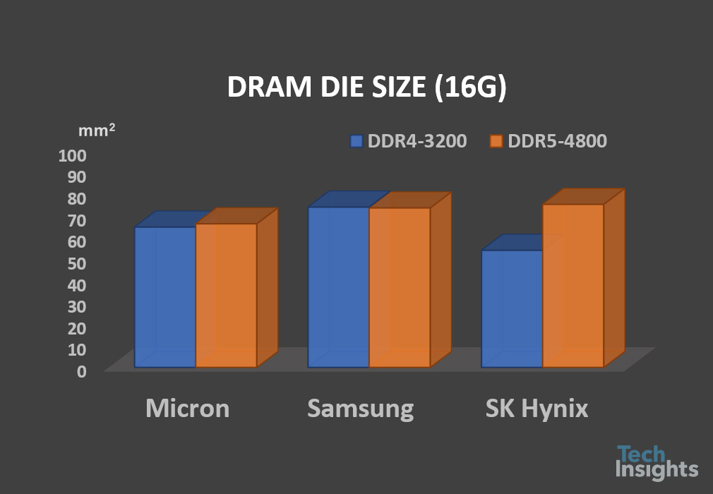
Figure 2. A comparison of 16Gb DRAM chip size from Micron, Samsung, and SK Hynix; DDR4-3200 vs. DDR5-4800.
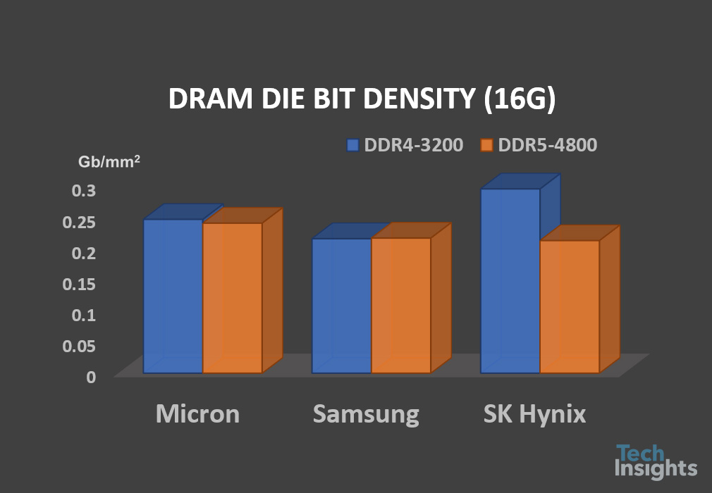
Figure 3. A comparison of 16Gb DRAM bit density from Micron, Samsung, and SK Hynix; DDR4-3200 vs. DDR5-4800.
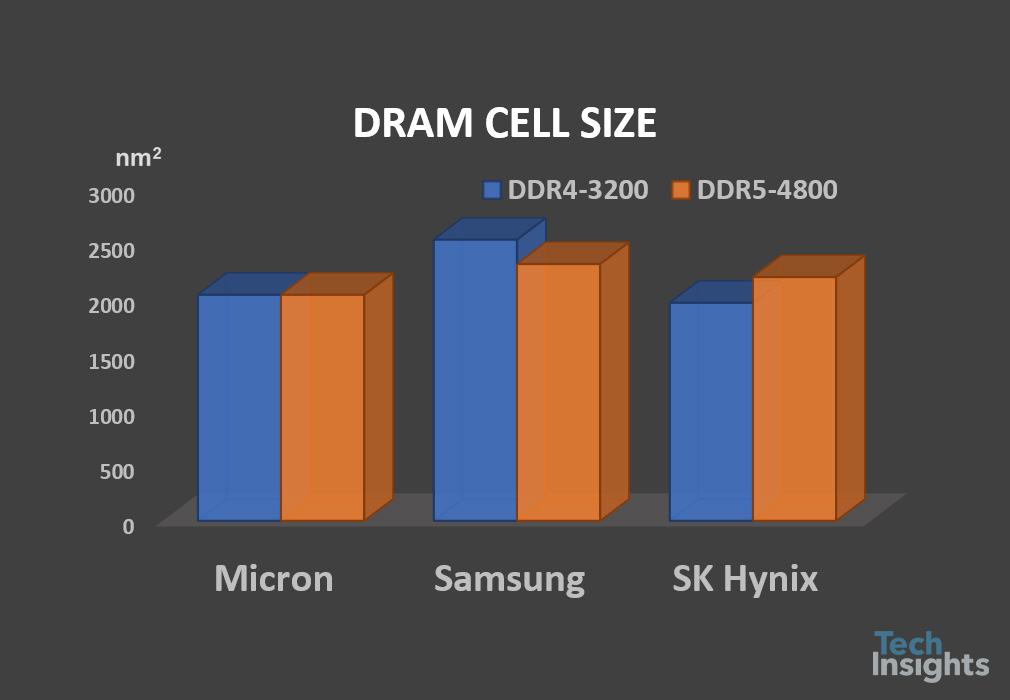
Figure 4. A comparison of 16Gb DRAM cell size from Micron, Samsung, and SK Hynix; DDR4-3200 vs. DDR5-4800.
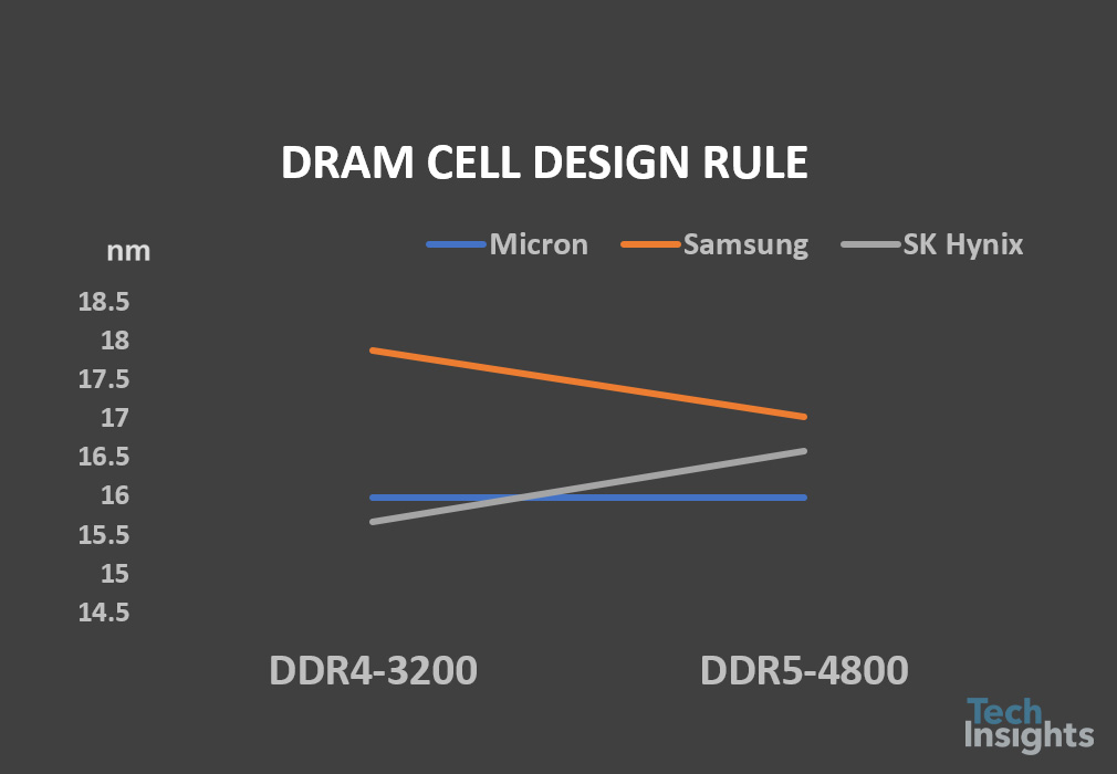
Figure 5. A comparison of 16Gb DRAM D/R from Micron, Samsung, and SK Hynix; DDR4-3200 vs. DDR5-4800.


