Cirrus Logic 55 nm PMIC Products Observed in the Market
Cirrus Logic are producing power management integrated circuit (PMIC) products with a 55 nm logic node, this is the lowest we have observed to date in the market. Two major innovations are being pursued by foundries for high logic density PMIC products: the migration from 200 – 300 mm wafers, and logic node process shrink to sub-90 nm.

Stephen Russell
Power management integrated circuit (PMIC)
Multiple vendors are pursuing this. Global Foundries offer 55 nm BCDLite® while both TSMC and STMicroelectronics have discussed 40 nm technology nodes. We have yet to observe ST or TSMC sub-90 nm BCD products in the market, however we know Cirrus Logic are working with Global Foundries on their 55 nm BCDLite® process offering 55 nm based PMIC products in some of todays leading smartphones.
Subscribe to TechInsights Blogs
Join our list to get the latest blog posts directly in your email.
We are starting to observe some of this technology in our recent teardowns of smartphones. An example being the Apple / Cirrus Logic 338S00817 part found on the board of the iPhone 13 Pro Max as shown in Figure 1 taken from our teardown report.
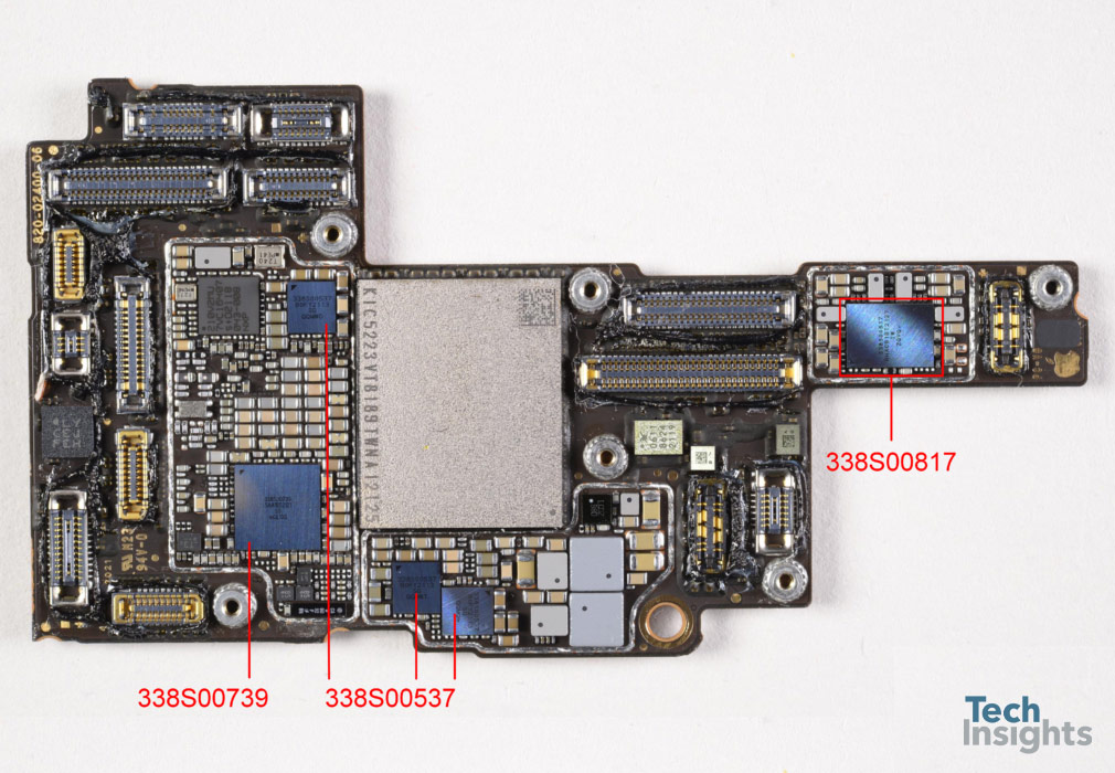
Figure 1. Location of 338S00817 and other Cirrus Logic Components on iPhone 13 Pro Max main board.
Apple have worked with Cirrus Logic on audio codecs and amplifiers for some time. (76% of Cirrus Logic’s revenue came from providing components to Apple in a recent fiscal quarter). The board also contains the 338S00739 audio codec and 3x 338S00537 audio amplifiers supplied by Cirrus Logic. This is the first time we have observed the 338S00817 part. It could be another audio amplification device or a broader application PMIC. Cirrus have recently stated a new focus on power conversion/control ICs and haptic drivers as well as announcing the acquisition of Lion Semiconductor for $335 million.
The Apple / Cirrus Logic 338S00817
Once the product’s packaging is removed it is clear from die markings this is a Cirrus Logic die (CLI1794B1) with 2021 date as seen in Figure 2, the entire die can be seen in Figure 3.
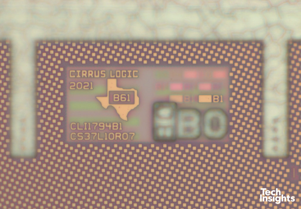
Figure 2. Cirrus Logic CLI1794B1 die marks.
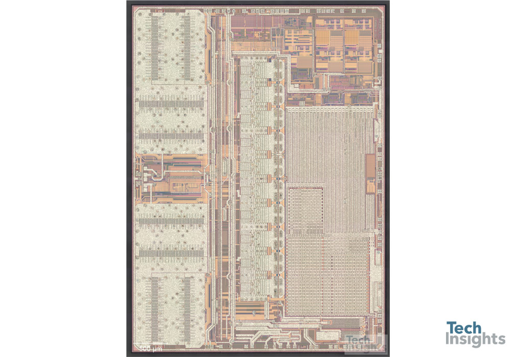
Figure 3. Cirrus Logic CLI1794B1 die.
Once deprocessed to the polysilicon level circuit analysis shows several major blocks to be present in Figure 4:
- Two digital circuit blocks taking up the central portion of the die area on the right-hand side.
- Several memory blocks below the digital blocks.
- Several analogue blocks above the digital blocks.
- Several power amplifiers based on LDMOS technology on the left-hand side of the die.
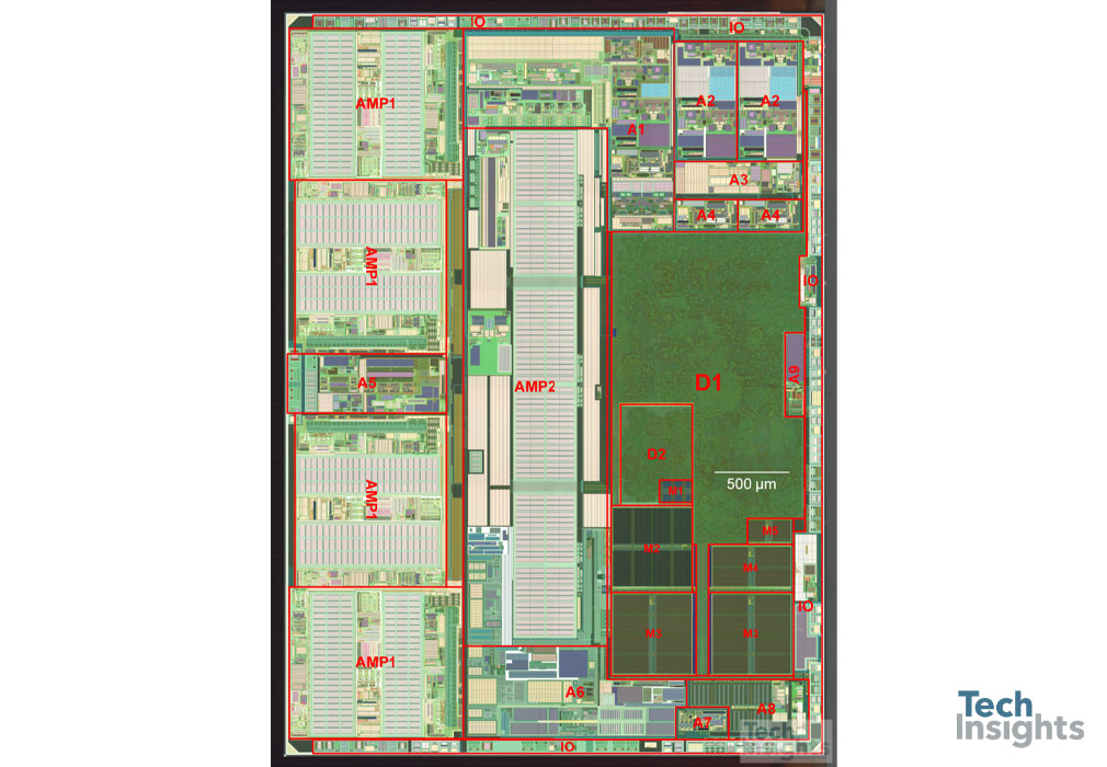
Figure 4. Circuit analysis of Cirrus Logic CLI1794B1 die.
Ensure you’re armed with the latest technical intelligence.
Sign up for a free trial today to see how the TechInsights Platform will help you.
Sample reports from this blog may be available with your free trial.
A scanning electron microscope (SEM) cross-section shown in Figure 5 cuts across the logic transistors and reveals a contacted gate pitch (CGP) of 260 nm. This places the logic node of this product comfortably sub-90 nm. Also, indicative of a sub-90 nm process is the use of nickel silicide for the ohmic contact process.
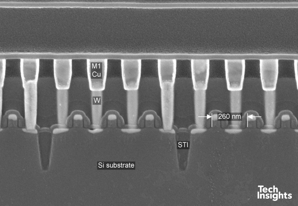
Figure 5. SEM cross-section of logic portion of Cirrus Logic CLI1794B1 die.
For comparison, a previous PMIC report analysed the Maxim PB38C die with 90 nm logic node. A cross-section of this device can be seen in Figure 6. The measured CGP of the logic portion was 430 nm.
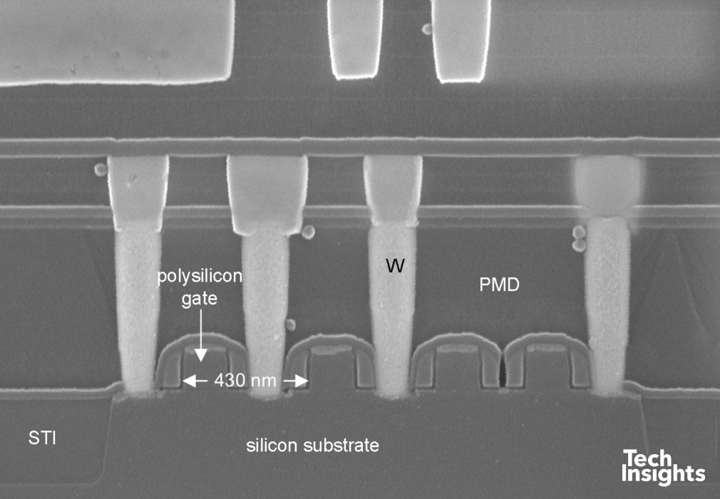
Figure 6. SEM cross-section of Maxim PB38C die.
We did not observe many bipolar devices across the CLI1794B1 die, although some candidate structures were present for example see the SEM image in Figure 7. This is potentially a bipolar junction transistor (BJT), although it could also be utilised as a diode with the collector contact grounded.
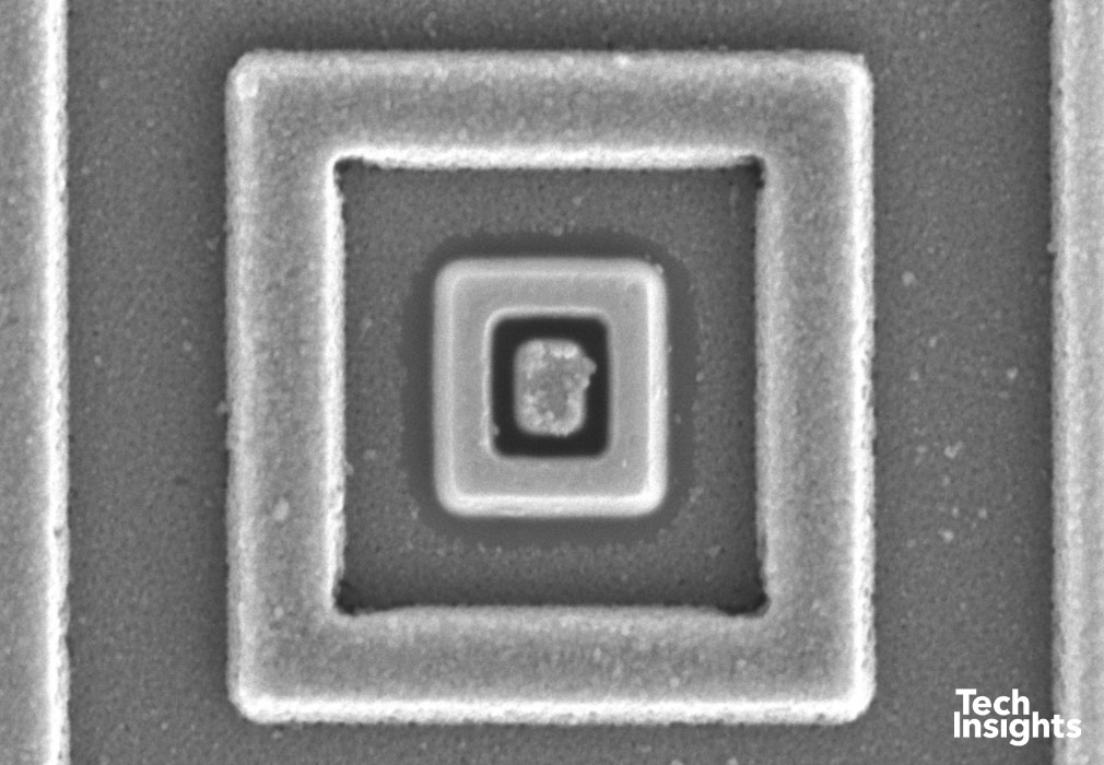
Figure 7. Potential bipolar junction transistor structure observed on CLI1794B1 die.
Further Examples
Another Cirrus Logic part we have found in recent smartphones is the CS35L41, a press release from 2019 quotes this part as having a 55 nm process technology. It is described as the industry’s smallest, low-power boosted smart audio amplifier. We have found this part in Xiaomi, Google and Sony phones since 2019. The die found within (CLI1755B2) is dated 2018 (See Figure 8).
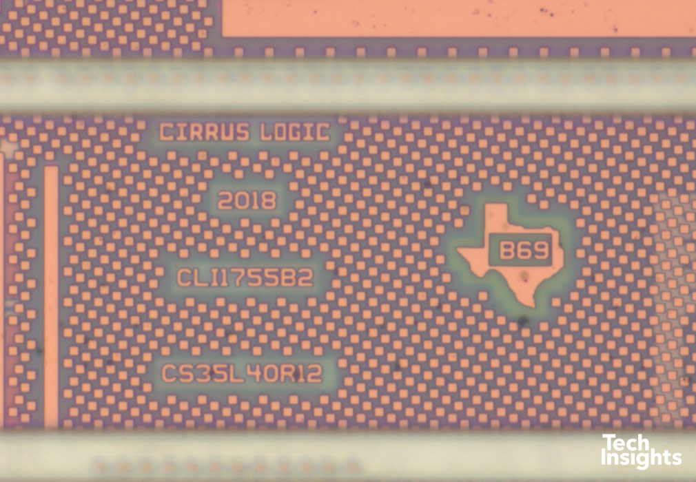
Figure 8. Cirrus Logic CLI1755B2 die marks.
Comparing the CGP of this part in an SEM cross-section we the similarity of the logic portion to the CLI1794B1 die. A CGP of 280 nm can be seen in Figure 9.
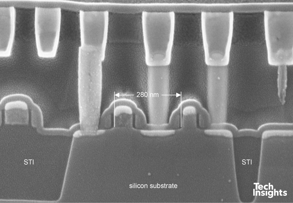
Figure 9. SEM cross-section of the Cirrus Logic CLI1755B2 die.
Another interesting point of comparison is the onsemi RSL10 Multi-Protocol Bluetooth System-on-Chip which we completed a Basic Floorplan Analysis of it in 2019. This part is known to use Global Foundries 55LPx technology (both this and the 55BCDLite® processes being an extension of their 55 nm platform). A circuit analysis of die deprocessed to polysilicon level is shown in Figure 10 contains the digital, memory and transceiver blocks one would expect from a Bluetooth SoC but lacks the power blocks present in the Apple / Cirrus Logic 338S00817 seen in Figure 4.
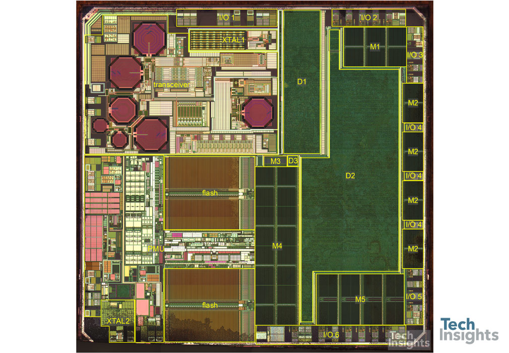
Figure 10. Colorado SV3 die from onsemi RSL10 Multi-Protocol Bluetooth System-on-Chip.
Given the evidence of a 55 nm logic node, presence of power blocks and statements in the press regarding Cirrus and Global Foundries working relationship it seems likely the 338S00817 and CS35L41 parts are manufactured using Global Foundries 55 BCDLite®. We also suspect further parts such as the Cirrus Logic CS35L38A found in Hauwei phones and CS35L45 from Asus, Meizu and Xiaomi phones to utilise this process.
EDIT: Since the orignal publication of this blog in the TechInsights' Platform, we have heard TSMC may in fact be the foundry who fabricated this PMIC. We know Cirrus Logic has worked with both TSMC and Global Foundries and we will keep monitoring their products and associated processes moving forward.
Further Examples
So why is a logic node of 55 nm important for a PMIC? It is after all an order of magnitude larger than the leading logic processes of today. The key to PMIC devices is balance, as well as having high-density logic which functions at fractions of volts, other parts of the same die will need to operate potentially into the tens of volts. Hence isolation between power and logic regions is crucial and not straightforward.
This process shrink allows the incorporation of more sophisticated functionality on to the die, it is most useful in mobile, wearable and IoT type products. We also see the incorporation of memory blocks onto the die.
PMIC devices can vary greatly in application, some products operate at hundreds of volts. In these cases, dense logic is not necessary as the large scale of the power blocks would d continue to dwarf any process shrink in the logic. Hence why companies such as STMicroelectronics’ BCD roadmap takes a dual approach ‘High Density’ and ‘High Voltage’ the second may employ a silicon on insulator (SOI) process and serve applications such as power transistor gate drivers.