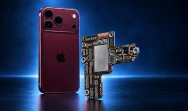
NXP Semiconductors 30V4E0 TSMC 28 nm eFlash Memory Floorplan Analysis

Share This Post
This is a Memory Floorplan Analysis (MFR) of the NXP Semiconductors 30V4E0 eFlash die with TSMC 28 nm HPL technology. Within the eFlash macro, memory subarrays take about 53% of the area, while memory array with array peripherals cover about 69% of the macro space.