Teardown-Backed Insights into How Hyperscalers Design Silicon for AI, HPC, and Cloud Scale
Decode Hyperscaler Architectures
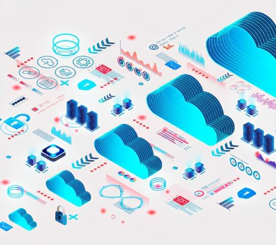
Hyperscalers are redefining compute architecture to meet the extreme demands of AI training, inference, and hyperscale cloud workloads. For fabless semiconductor companies, understanding how these systems are architected — and why — is critical to making the right design, performance, and packaging decisions.
This report delivers evidence-based analysis grounded in real silicon, revealing how leading hyperscalers optimize compute, memory, interconnect, and power at scale.

Frequently Asked Questions (FAQs)
- What is hyperscaler architecture?
-
Hyperscaler architecture refers to how large cloud providers design and integrate compute, memory, interconnect, and packaging to support massive AI, HPC, and cloud workloads at scale. These architectures prioritize performance, power efficiency, scalability, and cost in ways that increasingly influence the broader semiconductor ecosystem.
- How is this analysis different from public hyperscaler disclosures?
-
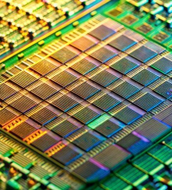
Public disclosures and conference presentations often describe architecture at a high level. This report is based on direct silicon teardown and reverse engineering, revealing what hyperscalers actually implement — including design trade-offs that are not visible in public materials.
- Who should read this report?
-
This report is designed for:
- Fabless chip and system architects
- Engineering and product leaders
- Semiconductor strategy and roadmap teams
- CTOs and executives focused on AI and cloud markets
If your organization designs silicon for AI, HPC, or hyperscale cloud infrastructure, this analysis provides critical context for decision-making.
- What types of workloads does the report focus on?
-
The analysis focuses on architectures optimized for:
- AI training and inference
- High-performance computing (HPC)
- Hyperscale cloud infrastructure
It examines how hyperscalers balance compute density, memory bandwidth, interconnect, and power efficiency to support these workloads.
- Does the report cover advanced packaging and chiplet strategies?
-
Yes. The report includes insights into advanced packaging, chiplet integration, and system-level design approaches used by hyperscalers to overcome scaling limits and improve performance and efficiency.
- How can fabless companies use these insights?
-
Fabless teams use this analysis to:
- Inform silicon and accelerator roadmap decisions
- Benchmark architectural trade-offs against hyperscaler designs
- Identify emerging design patterns and investment priorities
- Align engineering, product, and strategy teams around real-world architecture trends
- Is access restricted?
-
Yes. Access is provided to enterprise users with a corporate email address. This ensures the analysis remains available to professionals working in semiconductor, AI, and cloud infrastructure fields.
- How current is the analysis?
-
The report reflects the latest available silicon and architecture data analyzed by TechInsights. As hyperscaler designs evolve, TechInsights continuously updates its analysis to reflect new architectures and integration approaches.