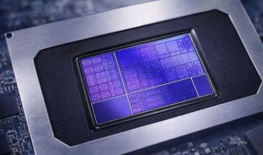
SK hynix H5CGD8MHBD-X021 D1a EUV 24Gb DDR5 DRAM Memory Floorplan Analysis
Share This Post
This is a Memory Floorplan Analysis (MFR) of the SK Hynix MDHD5C21001 die found inside SK Hynix H5CGD8MHBD-X021. The SK Hynix H5CGD8MHBD-X021 was extracted from the G.Skill Trident Z5 RGB 24 GB DDR5 DRAM. The die was manufactured by SK Hynix using its 1a nm generation stacked DRAM CMOS process incorporating five back end of line (BEOL) interconnect metal layers (one aluminium (Al), three copper (Cu), and one tungsten (W)) with W-filled via 4s and via 1s, Cu-filled via 3s and via 2s, an Al redistribution layer (RDL), bit line (BL) under capacitors, and a buried word line (WL) forming the gate of the buried cell array transistor (BCAT). Extreme ultraviolet lithography (EUV) is used at metal 1 and the storage node landing pad (SNLP) level. The BLs and WLs are at pitches of 44.5 nm and 39.5 nm, respectively.


