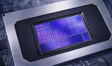
SK hynix H58G66AK6H-X132 1z nm 16 Gb LPDDR5 DRAM Memory Floorplan Analysis
Share This Post
This report presents a Memory Floorplan Analysis of the SK Hynix MDHD5E_20104 die found inside SK Hynix H58G66AK6H-X132. The H58G66AK6H-X132 was extracted from the Apple iPhone 15 Pro 5G smartphone. The die was manufactured by SK Hynix using its 1z nm generation stacked DRAM CMOS process incorporating five back end of line (BEOL) interconnect metal layers (one aluminium (Al), three copper (Cu), and one tungsten (W)) with W-filled via 4s and via 1s, Cu-filled via 3s and via 2s, an Al redistribution layer (RDL), bit line (BL) under capacitors, and a buried word line (WL) forming the gate of the buried cell array transistor (BCAT). The BLs and WLs are at pitches of 47.4 nm and 42.0 nm, respectively.


