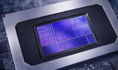
Renesas R7F702301BEBBA-C TSMC 28nm eFlash Memory Floorplan Analysis
Share This Post
This report is a Memory Floorplan Analysis (MFR) of the embedded flash memory on the Renesas R7F702301B die found inside Renesas R7F702301BEBBA-C. It is manufactured using a process featuring double-layer passivation, 10 layers of metal interconnect (1 aluminium (Al), 9 copper (Cu)), tungsten (W) contacts, shallow trench isolation (STI), and high-K metal gate (HKMG) transistors. The minimum observed metal and contacted gate pitches are 90 nm and 123 nm, respectively. These measured critical dimensions, along with the observed features of the transistors, suggest that the R7F702301B die was manufactured on 300 mm wafers using the TSMC 28 nm HPL HKMG CMOS process. The die features 8 MB of code flash realized using split gate metal oxide nitride oxide silicon (SG-MONOS) flash cells.


