Logic Analysis Blog
Qualcomm dual-sourced Snapdragon 8(+) Gen1 SOC
TechInsights’ confirms TSMC N4 is a true optical shrink from N5 node

Richard Li

John Boyd
For the first time in recent memory, Qualcomm has dual-sourced their Snapdragon 8(+) Gen1 SoC with both Samsung (4LPX) and TSMC (N4). This has allowed us at TechInsights to compare a common design manufactured by two different foundries.
Our earlier report indicated that TSMC’s N4E process, an early version of TSMC’s N4 process used in Mediateck’s Dimensity 9000, came with a mask reduction but no shrinkage. You may wonder if TSMC’s N4 process is a true optical shrink from N5? Now, we have the answer:
In our recently released First Look Report of Snapdragon 8(+) Gen1 SoC on TSMC N4, we confirmed that the TSMC N4 technology in which the Snapdragon 8(+) Gen1 SoC was manufactured is a true optical shrink from the TSMC N5 node.
Further shrinks have been found with the bitcells (smallest being a 4% shrink), while other technology features are shared with the previous technology generations and summarized in TechInsights’ First Look Report (available now to our subscribers)
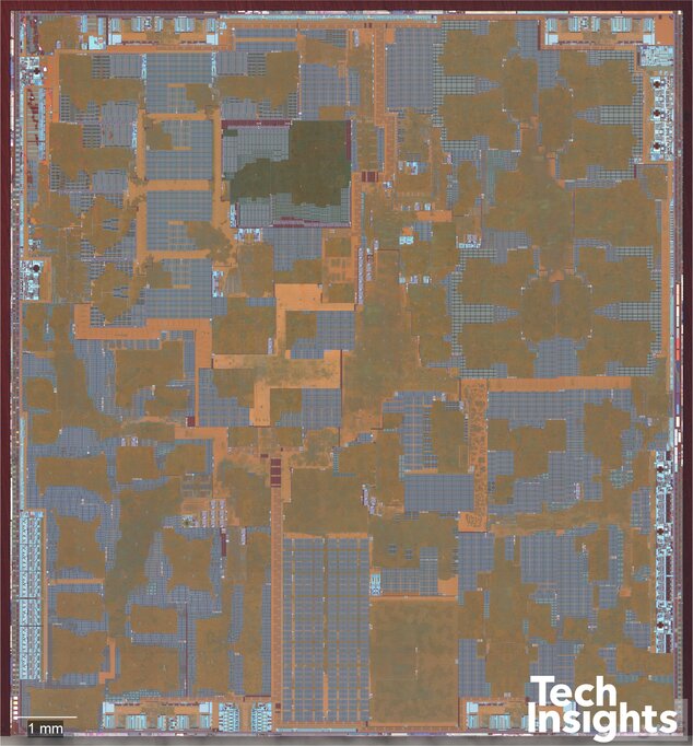
Figure 1:Floorplan image of the Qualcomm Snapdragon 8 Gen 1 SoC
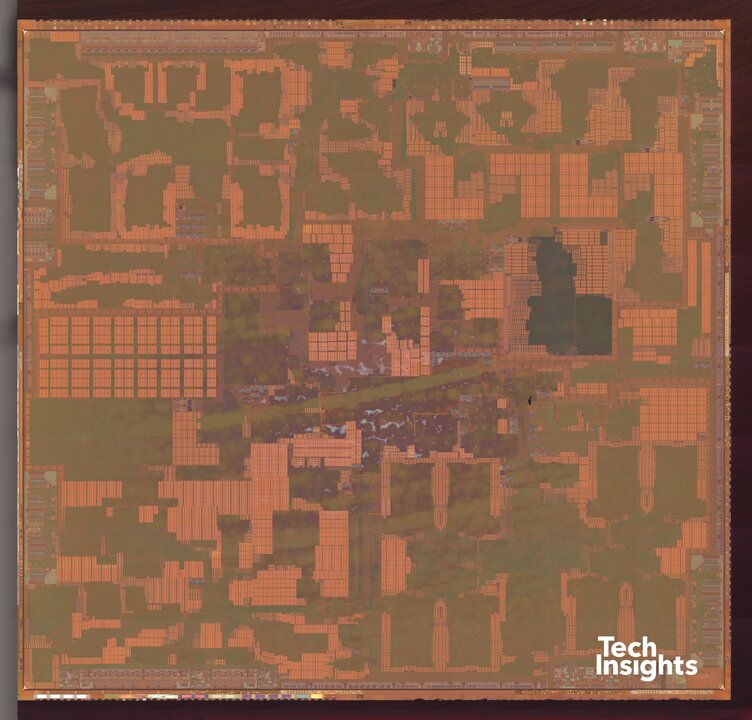
Figure 2: Floorplan image of the Qualcomm Snapdragon 8+ Gen1 SoC
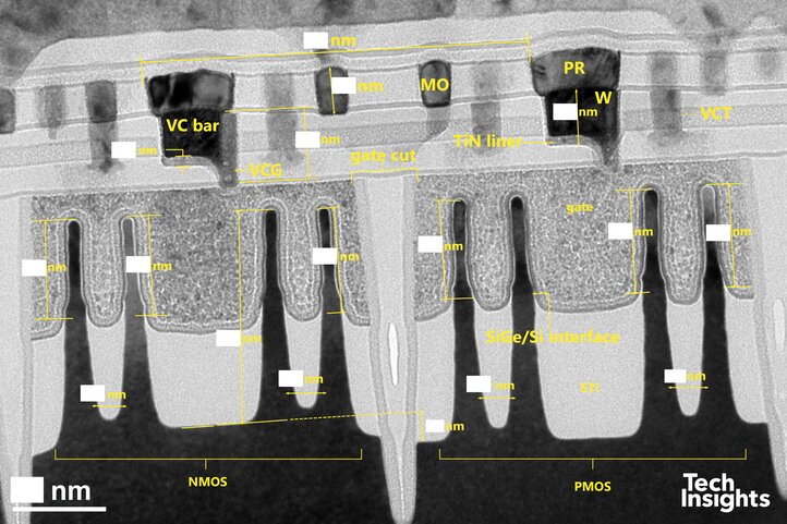
Figure 3:TEM Cross Section through the high-density Library Logic Block
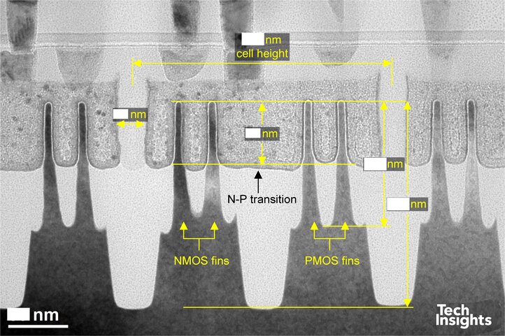
Figure 4: TEM Cross Section through the high-density Library Logic Block
Want to know more? Subscribe to TechInsights Logic Process Channel to see the full report. After becoming a subscriber, you can also check out our:
- First Look report of Snapdragon 8 Gen1 manufactured in Samsung’s 4LPX technology
- Advanced CMOS Essentials report of Snapdragon 8 Gen1 manufactured in Samsung’s 4LPX technology
- Comparison between Samsung’s Exynos 2200 4LPE (a major process node change with pitch scaling) and 4LPX (essentially a 5LPE technology) technologies