Contributed by: Sinjin Dixon-Warren, PhD
The emergence of gallium nitride (GaN) technology in the USB-C chargers is a new trend in the semiconductor market. Over the past year, TechInsights has found GaN technology from Navitas and from Power Integrations in various USB chargers, as published in various recent blogs and articles. The use of GaN promises increased efficiency, reduced thermal losses and a smaller form factor, as compared to silicon-based technologies.
Internally these chargers are compact switching power supplies that efficiently converts line AC into a 5 V DC output. The input AC is first converted to high-voltage DC. The DC is chopped at high frequency and fed into a small flyback transformer. The output of the transformer is converted to low-voltage DC, filtered, and provided as the 5 V output through the USB port. A feedback mechanism regulates the chopping frequency to keep the output voltage stable. Name-brand chargers use a specialized control IC to run the charger, while cheaper devices replace the IC with a low-quality feedback circuit.
The latest entrant to the GaN-based USB chargers is Innoscience. Innoscience (Zhuhai) Technology Co., Ltd. was founded in December 2015, in the Zhuhai National Hi-Tech District. They have established China’s first mass production line for 8-inch GaN-on-Si power devices. Innoscience apparently provides a wide range of solutions including 30 V - 650 V GaN-on-Si power devices and 5G RF devices.
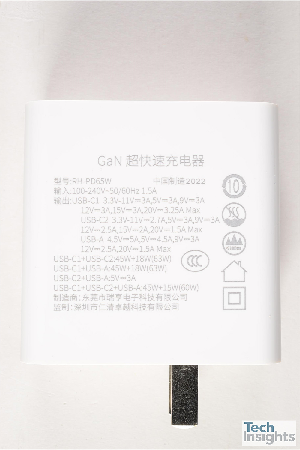
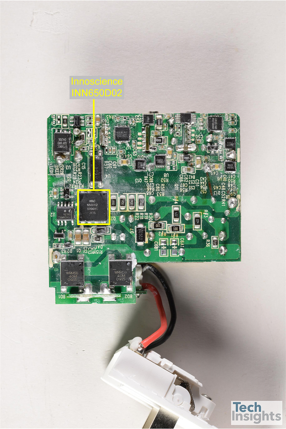
We have found the Innoscience INN650D02 in the ROCK RH-PD65W 65 W (20 V, 3.25 A) USB-C wall charger, manufactured by Shenzhen Renqing Excellent Technology Co. Ltd. The INN650D02 is a 650 V GaN enhancement-mode power transistor, with an RDSON of 200 mW, according to the datasheet.
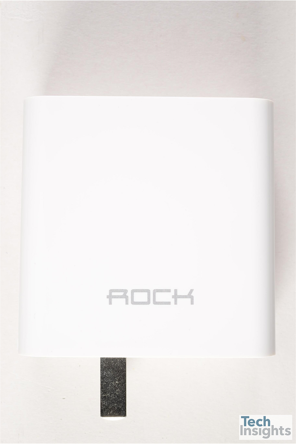
Figure 1 and Figure 2 show the front and back of the ROCK RH-PD65W, which is 6.0 cm x 6.0 cm x 2.9 cm, excluding the plug pins. It provides a maximum power density of 10.2 W/in3, which is a bit below average for the chargers recently analyzed by TechInsights. The top side of the main PCB found inside the RH-PD65W is shown in Figure 3. The INN650D02 is seen near the middle of the board.
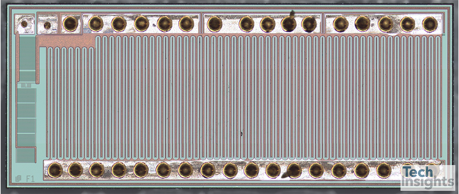
The Innoscience INN650D02 was removed from the PCB for further analysis. Figure 4 presents a plan-view X-ray of the INN650D02 package. A single die is seen in the middle of the package, connected by bond wires to source (S), drain (D) and gate (G) pins. An SK monitoring pin is also provided. Decapsulation in the TechInsights labs revealed the die, which has a “F1” marking in the bottom left corner, as shown in Figure 5. The drain pads are located along the bottom edge of the die, while the source and gate pads are located at the top edge. The high electron mobility transistor (HEMT) gate fingers run vertically across the die.
Figure 6 shows a SEM cross-sectional view of the INN650D02 F1 die structure. The device uses four levels of metallization, including a metal 0 substrate contact layer and a metal 1 gate contact layer, on a GaN-on-Si substrate. The gates are formed as mesas of likely P-type GaN.