Posted: February 7, 2019
Contributing Authors: Sinjin Dixon-Warren, PhD
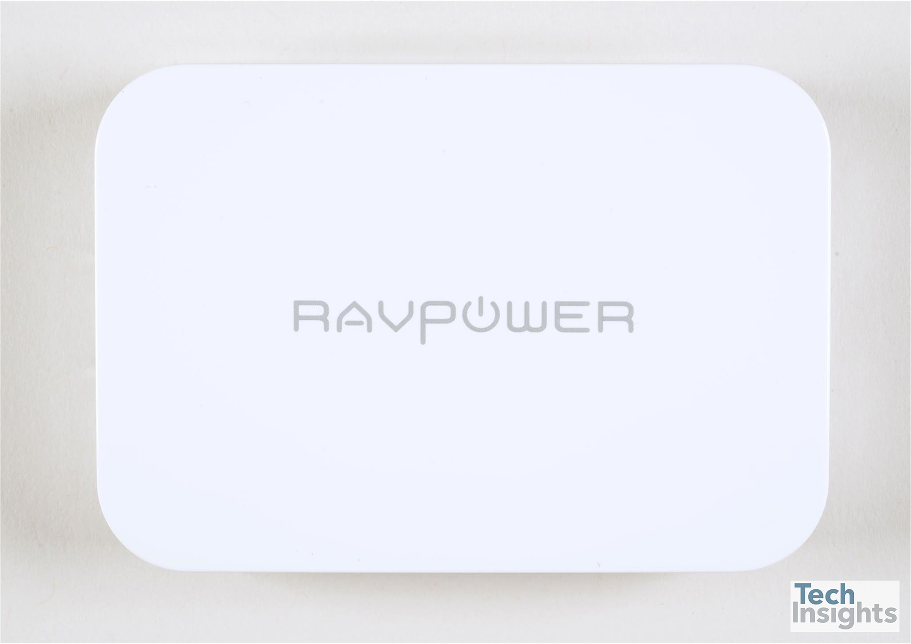
Figure 1 – RAVPower RP-PC104 USB-C Charger
One of the primary emerging applications for 650 V gallium nitride (GaN) power High Electron Mobility Transistors (HEMT) is likely to be compact, mobile, USB-C fast-chargers. An internet search for “GaN laptop charger” indicates that several companies are targeting this market, including RAVPower, Anker, FINsix and Made in Mind (Mu One). The RAVPower RP-PC104 USB-C charger, shown in Figure 1, is currently in volume production.
GaN has been a major focus of power electronics research and development for several years. This is due to the physical properties that theoretically allow a GaN transistor to exceed the performance specifications of a silicon power MOSFET, in terms of breakdown voltage, on-state resistance (RDS,ON), gate capacitance (Qg), and other performance parameters. The main challenge has always been obtaining high quality GaN substrates at a reasonable price. Bulk GaN wafers are very expensive and are only available up to 2” diameter. GaN epitaxial layers can be grown on silicon carbide (SiC), but the cost is also high for this method.
More recently, it has become possible to grow device-quality GaN on Si substrates, which allows for the formation of lateral transistor structures, but not for vertical transistors. The availability of GaN-on-Si at reasonable cost has been particularly disruptive in the market, since it enables conventional silicon processing tools to be used for processing the GaN-on-Si wafers.
In 2016 Chipworks (now TechInsights) analyzed the Avogy Zolt laptop charger, which was believed at the time to be based on GaN Technology. To our surprise, we found the Zolt contained a SiC die likely fabricated by Cree. A subsequent PntPower.com blog discusses the 4 reasons why Avogy and Finsix put SiC in their Charger. Essentially, although GaN is theoretically better than SiC for this application, in 2016 reliable 600 V GaN technology was not available in volume production. Although SiC was more expensive, it was available and working, and it was the best option at the time for building a working compact charger. According to PntPower.com FINsix also used SiC in their DART charger.
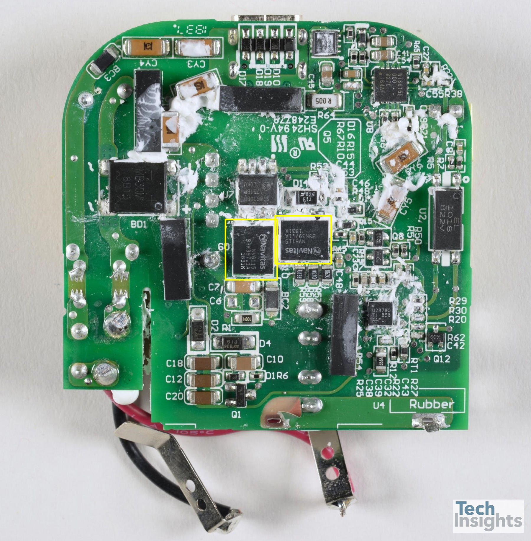
Figure 2 – RAVPower RP-PC104 USB-C Charger Main PCB
RAVPower RP-PC104-W Charger
TechInsights recently procured the RAVPower RP-PC104-W charger. Our teardown has found that it contains two Navitas NV6115 GaN-based power IC’s, indicated by the yellow boxes in Figure 2, that are mounted onto the main PCB. This is the first commercial product analyzed in our lab that is known to contain GaN power technology. According to the datasheet the NV6115 is a 650 V GaNFast Power IC with 170 mΩ RDS,ON and a 2 MHz operation frequency.
Table 1 provides a full list of the design wins found inside the RAVPower RP-PC104-W. In addition to these IC’s the RP-PC104-W contained several large capacitors and an inductor.
| Manufacturer Name | Part Number | Device Type |
|---|---|---|
| Navitas Semiconductor | NV6115 | GaN Power IC |
| Diodes Inc | MSB30M | Power Rectifier |
| Vanguard International | VS3506AE | P-Channel FET |
| Silicon Laboratories | Si8610BB-B-IS | Digital Isolator |
| Everlight | EL1018-G | Photocoupler |
| Texas Instruments | UCC28780RTE | UCC28780 High Frequency Active Clamp Flyback Controller |
| Infineon | BSC098N10NS5 | Power MOSFET |
| Weltrend Semiconductor | WT6615F | USB Power Delivery (PD) controller |
Table 1 – RAVPower RP-PC104 Design Wins
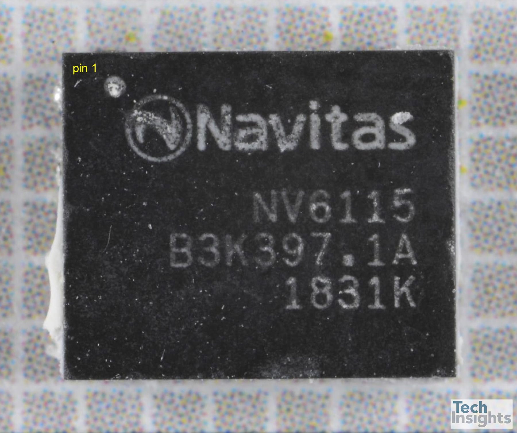
Figure 3 – Navitas NV6115 Package Top
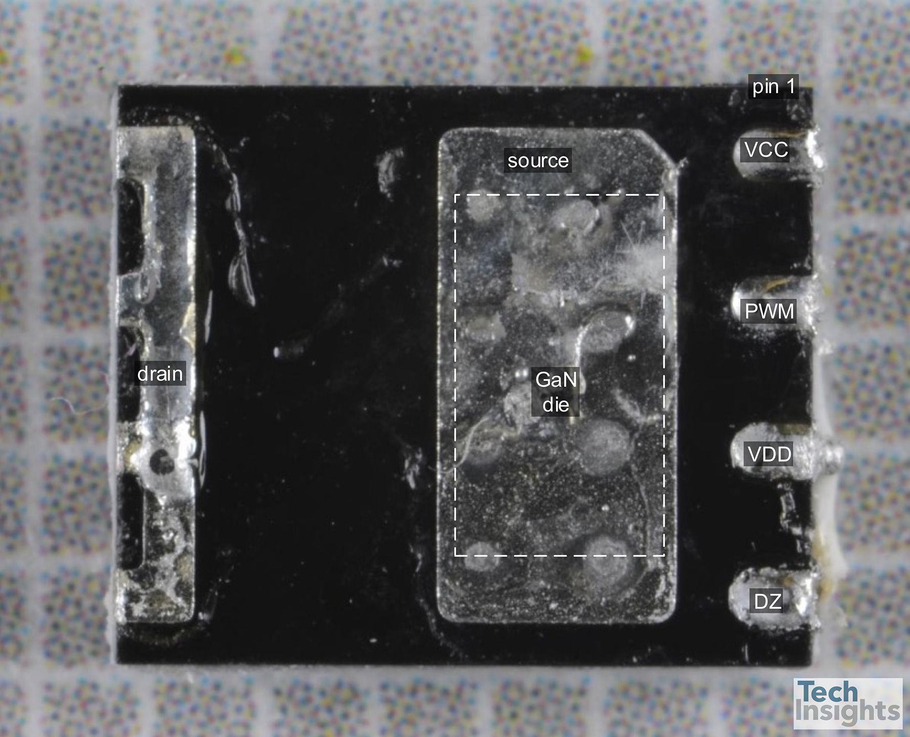
Figure 4 – Navitas NV6115 Package Bottom
Navitas NV6115 Packaging
The Navitas NV6115 features a 5.0 mm x 6.0 mm x 0.85 mm thick quad flat no-lead (QFN) package, shown in Figure 3. The backside of the package shows a large source and drain terminal, plus separate pins for power (VDD), ground (VCC), pulse width modulation input (PWM) and VDD setting voltage (DZ), shown on the bottom side of the package in Figure 4.
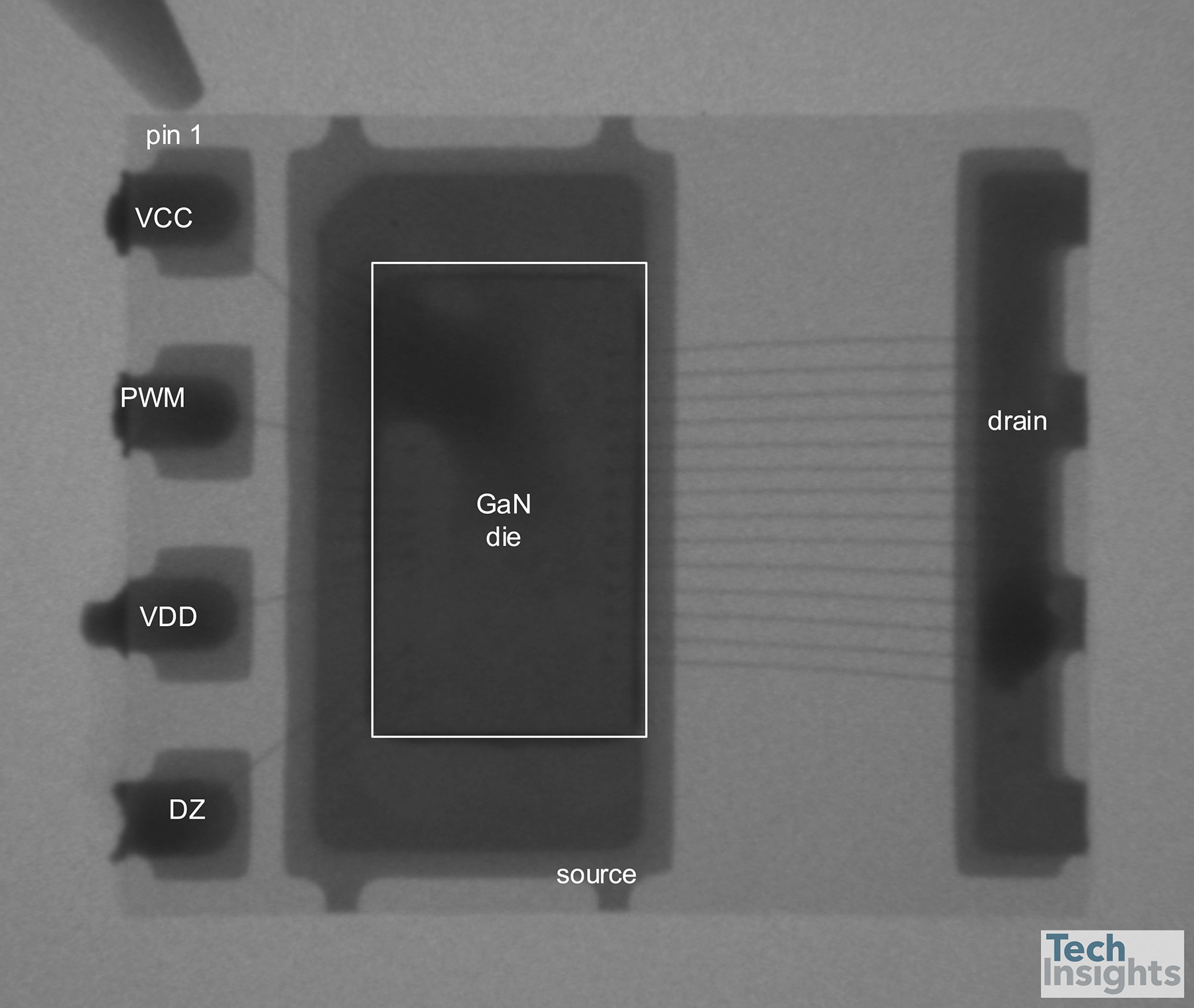
Figure 5 – Navitas NV6115 Package X-Ray
Figure 5 is a top side plan-view X-ray of the Navitas NV6115. The source and drain pin connections are wire bonded with multiple wires to the GaN die. The VCC ground, PWM, VDD power and DZ connection are wire bonded to the die with single wires.
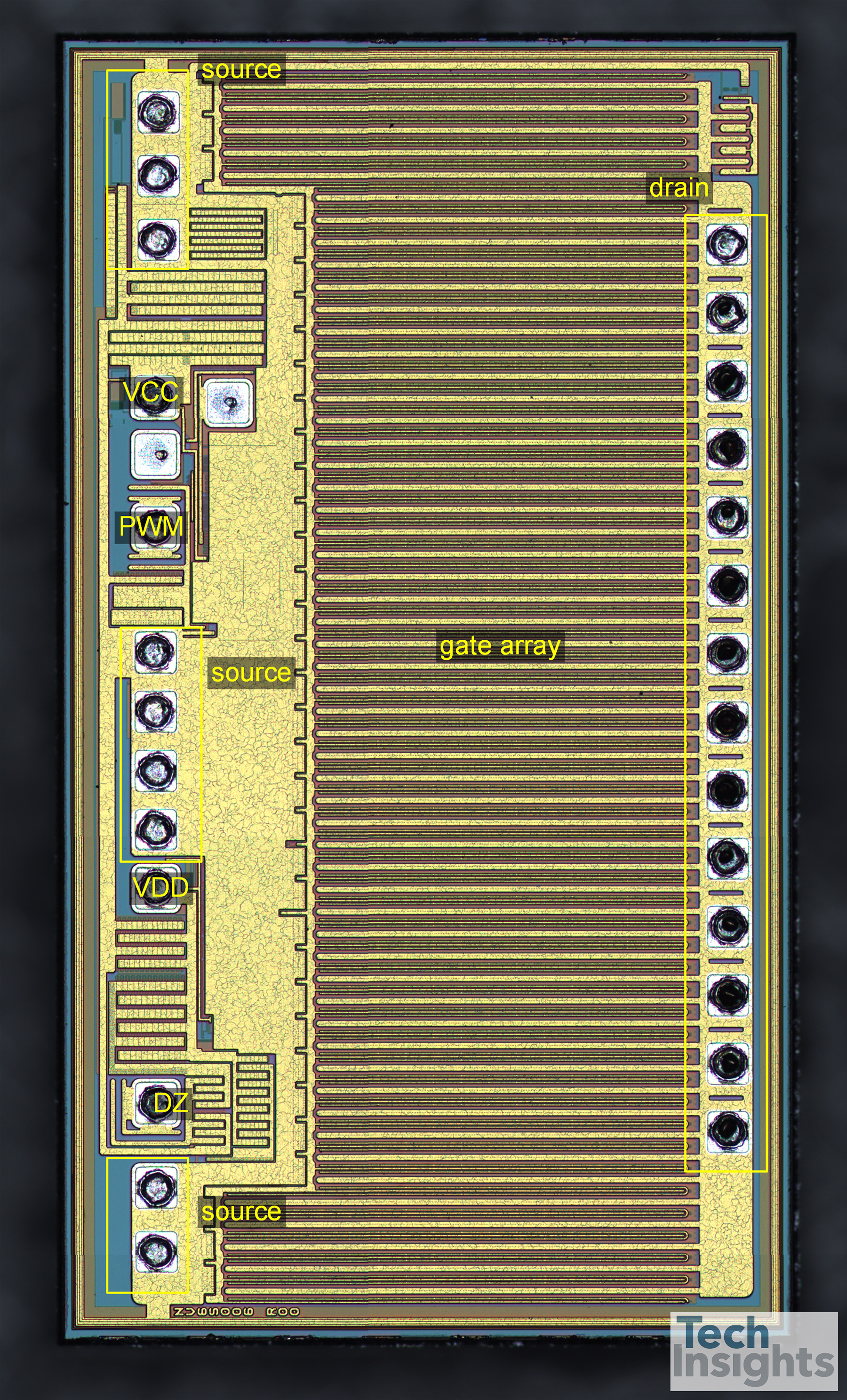
Figure 6 – Navitas NV6S006 R00 Die
Figure 6 shows a high-resolution photograph of the GaN-on-Si die, with NV6S006 R00 die markings, that is found inside the Navitas NV6115 Package. The central portion of the die contains the high electron mobility transistor (HEMT) gate array.
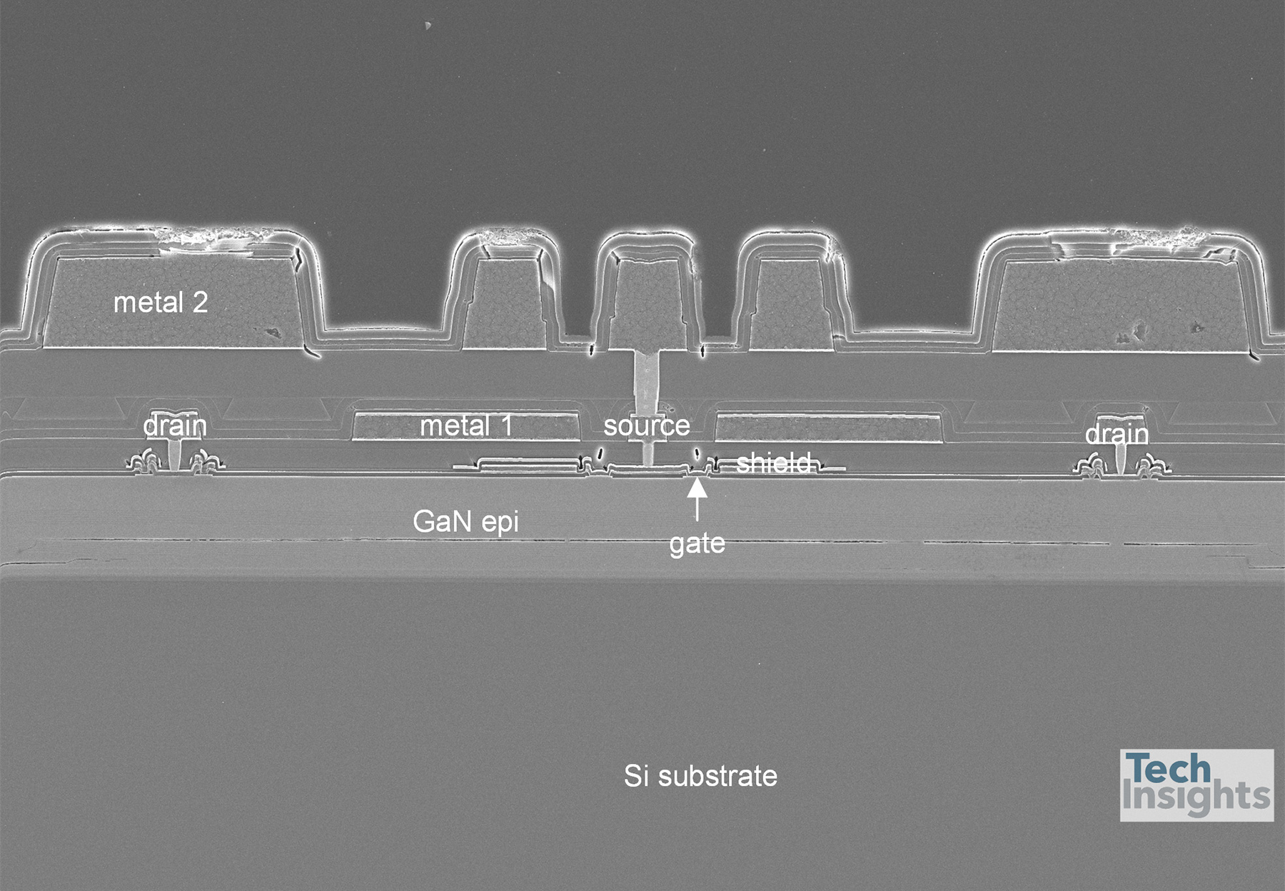
Figure 7 – Navitas NV6S006 R00 Die General Structure
The NV6S006 R00 die was subjected to cross sectional analysis in our lab. Figure 7 shows the general structure of the die, which features two layers of aluminum interconnect metal formed over the GaN-on-Si substrate. A metal 0 layer is used to form the transistor source, drain connection and the gate. An additional metal layer is used to form a metal shield that extends from the gate towards the transistor drain connection.
TechInsights has recently completed analysis of a related Navitas device, the NV6117, which comes in the same 5 mm x 6 mm QFN package, but features a lower 120 mΩ RDS,ON. Detailed analysis of this device is available through TechInsights Power Semiconductor subscription. Our analysis found that the NV6117 die features HEMT-based control circuitry. Navitas claims to be first to market with a GaN power IC with integration of logic, analog and power onto a single GaN IC.
This UBS-C charger is a typical example of Navitas’ market penetration strategy. They have designed a GaN IC with a driver, some control but mainly protection systems integrated making their device easy to integrate. Aftermarket consumer power supply makers do not have an army of power electronics designers anymore. The converters have quite a standard topology and have not evolved much in the past 5 years. Manufacturers would need to recruit new engineering talent to rebuild a power converter design task force and be able to quickly release GaN-based power supplies. Navitas has well understood the situation, and so they propose a complete application design, ready to implement with few or no tweaks. The Active Clamp Flyback is part of the design they have proposed, and it has probably been sold to several consumer power supply makers like Anker, Aukey, Made in Mind, etc. Navitas facilitates the designer’s job as much as possible, enabling them to sell their products. It seems to be a winning strategy to kickstart GaN production and Navitas revenues.
You may also be interested in reading our recent posting on the STMicroelectronics BCD92 process.
TechInsights’ full analysis of the RAVPower RP-PC104 USB-C charger referenced in this post is included in our new Power Semiconductor subscription.
The purpose of this subscription is to provide access to our analysis of new technologies in the power semiconductor market, including GaN, SiC, plus Si MOSFET and IGBT devices. It also includes our library of BCD technology reports.
Learn more about the TechInsights Power Semiconductor subscription.


