World’s First 1 Gb 28 nm STT-MRAM Product - by Everspin
Everspin’s new 1-Gigabit (Gb) Spin Torque Transfer Magneto-resistive Random Access Memory (STT-MRAM) device with a 28 nm process is the world’s first 1 Gb STT-MRAM product. This 4th generation MRAM technology release is a standalone market leader. Its only industry peers, Intel and Micron XPoint Memory, are developing MRAM, ReRAM, and FeRAM memory devices for embedded non-volatile memory (eNVM), rather than discrete emerging memory chips.
According to Everspin, their leading STT-MRAM memory products are being developed for “infrastructure and data center providers to increase the reliability and performance of systems where high-performance data persistence is critical by delivering protection against power loss without the use of supercapacitors or batteries.”
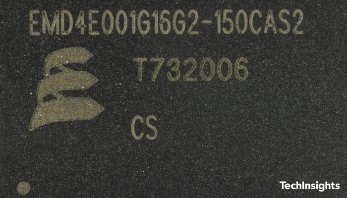
Everspin and GlobalFoundries (GF) have been partners since their 40 nm MRAM development and fabrication process. TechInsights is now extracting analysis from their 28 nm CMOS (Complementary metal–oxide–semiconductor) process and the technology architecture of the 1 Gb STT-MRAM. We extracted the 1 Gb STT-MRAM die from EMD4E001G16G2, the newest and highest capacity stand-alone spin-transfer torque random access memory device.
TechInsights Emerging & Embedded Memory subject matter experts agree that the 1Gb ST-DDR4 product interface shows expansive system design applications such as:
- storage
- computing, and networking
- internet of things (IoT)
- artificial intelligence (Ai)
- data persistence in power supply conditions
What is Everspin striving to accomplish with these developments?
Compared to the previous 256 Mb 40 nm STT-MRAM EMD3D256M DDR3, MRAM memory cells dramatically reduced in size to 0.0396 µm2 with 110 nm WL pitch and 180 nm BL pitch, which is just 25 % cell size from the previous one. Bit density reached to 9.75 Mb/mm2. Everspin and GF keep the MRAM location between M3 and M4, although BEOL interconnection metal layers increased from five to seven (Figure 1).
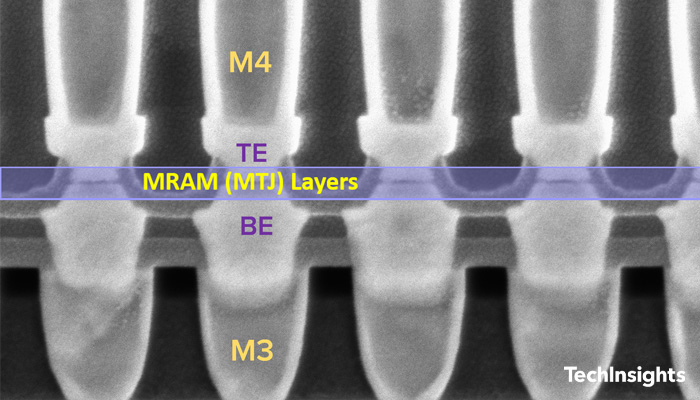
Figure 1. Everspin 4th gen. 1Gb MRAM layers integrated between M3 and M4
Everspin has four different MRAM types of memory products released on the commercial market, including Toggle-mode MRAM (1st generation, Chandler fab.) and STT-MRAM (2nd ~ 4th generation, GF fab.). Table 1 shows a comparison of device technology and die design with STT-MRAM.
| Items | Everspin 2nd Gen. MRAM (DDR3) |
Everspin 3rd Gen. MRAM (DDR3) |
Everspin 4th Gen. MRAM (DDR4) |
|---|---|---|---|
| Product Example | EMD3D064M DDR3 ST-MRAM |
EMD3D256M DDR3 ST-MRAM |
EMD4E001G DDR4 ST-MRAM |
| Die Size | 65.3 mm2 (11.15 mm x 5.86 mm) |
100.1 mm2 (12.12 mm x 8.26 mm) |
105.1 mm2 (12.29 mm x 8.55 mm) |
| Technology Node | 90 nm | 40 nm | 28 nm |
| Memory / Die | 64 Mb | 256 Mb | 1,024 Mb (1 Gb) |
| Bit Density | 0.98 Mb/mm2 | 2.56 Mb/mm2 | 9.75 Mb/mm2 |
| Cell Size | 0.387 µm2 | 0.156 µm2 | 0.0396 µm2 |
| Pitch (WL/BL) | 530 nm / 730 nm | 150 nm / 520 nm | 110 nm / 180 nm |
| MTJ | In-plane MTJ | pMTJ | pMTJ |
| MRAM Integration | Between M3 and M4 | Between M3 and M4 | Between M3 and M4 |
| # Metals | 5 | 5 | 7 |
Table 1: A comparison of STT-MRAM devices from Everspin Technologies, including in-plane MTJ and pMTJ
Among STT-MRAM products, the 2nd generation STT-MRAM devices use a MgO-based in-plane MTJ, while the 3rd and 4th generation STT-MRAM devices use a perpendicular MTJ (pMTJ) technology. The pMTJ STT-MRAM technology is common nowadays for MRAM players such as Everspin, Samsung, Sony, and Avalanche.
What are competitors doing in this space?
IBM to reveal the world's first 14nm STT-MRAM node
IBM announced that during the 2020 IEEE International Electron Devices Meeting (IEDM 2020), that is now virtual, its researchers will reveal the first 14 nm node STT-MRAM. IBM says that efficient and high-performance STT-MRAM systems will help to address memory-compute bottlenecks in hybrid cloud systems.
Avalanche Technology and Mouser Electronics Announce Global Distribution Agreement
Mouser will offer Avalanche’s STT-MRAM products for Industrial Automation & Internet of Things applications.
Numem to supply its STT-MRAM to a NASA AI core project
High-performance STT-MRAM developer Numem announced that it was selected for a NASA AI project, for which the company will supply its Numem NuRAM MRAM-based Memory. Numem says its memory enables a 2-3x smaller memory area and 20x to 50x lower standby power compared to SRAM.
We expect the MRAM structure consists of the MgO tunnel barrier-based pMTJ materials combined with multiple layered structure including free layers, reference layers, SAF, pinning layer, transition layer, spacer, and seed layer. Please stay tuned on TechInsights’ further analysis on this!
Find content like this and more in the TechInsights Platform. Sign-up for free today.


