TSMC 22ULL eMRAM Die removed from Ambiq™ Apollo4
Another Disruptive Technology on Embedded Memory!
Another disruptive product on embedded Memory (eMemory) has been arrived and quickly reviewed! TSMC has successfully developed and commercialized 22 nm eMRAM products with STT-MRAM technology and device integration. TechInsights removed TSMC eMRAM die from Ambiq™ Apollo4 Blue MCU (Parent Product: Fitbit Luxe Fitness Band). The Apollo4 SoC (Package Markings: 2M AMA4B) is the 4th generation system processor solution built upon Ambiq’s proprietary Subthreshold Power-Optimized Technology (SPOT) platform.
This subscription-based service provides companies with competitive analysis revealing the process design innovations of today’s technology market leaders
TechInsights' Emerging and Embedded Memory experts agree that the TSMC 22ULL eMRAM shows expansive system design applications such as:
- IoT (internet of things) Devices
- Battery-powered endpoint devices
- Wearable Devices
- Efficient non-volatile memory for code and data
- Automotive
- MCU (microprocessor)
- Server
- Analog Controllers
- Sensor Hubs
Ambiq™ Apollo4 and TSMC 22ULL Process Enabling High-Intelligence Without Sacrificing Battery Life on Cutting Edge IOT Devices
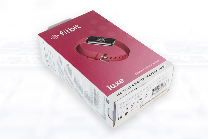
Figure 1. Fitbit Luxe fitness band packaging
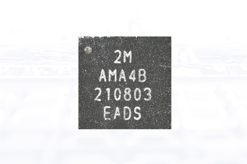
Figure 2. Ambiq™ Apollo4 Blue MCU package
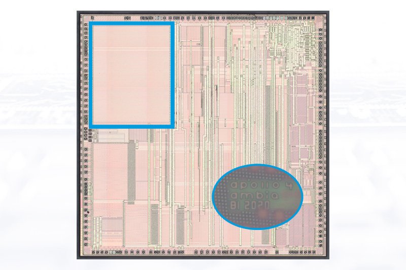
Figure 3. Ambiq™ Apollo4 Blue MCU die photo
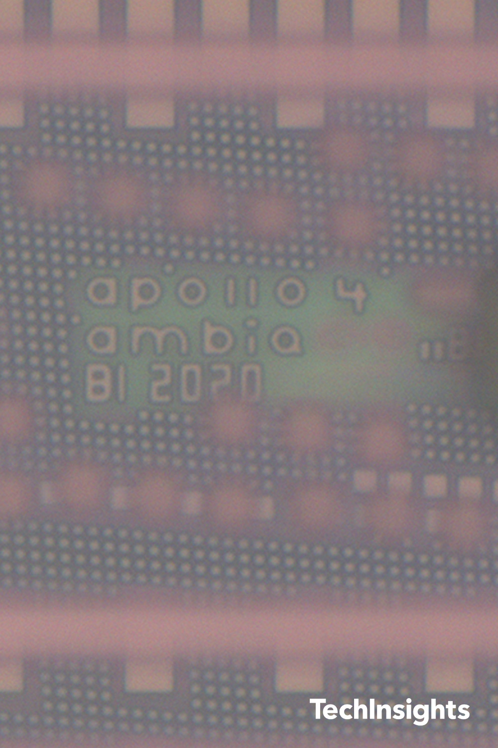
The Apollo4 SoC is implemented on the TSMC 22 nm Ultra-Low-Leakage (22ULL) HKMG Gate-last process and based on a 32-bit Arm Cortex-M4 processor with FPU and Arm Artisan physical IP, achieving 3 μA/MHz from MRAM with low deep sleep current modes. TSMC 22ULL eSTT-MRAM is essential to support on-chip code storage for MCU functions to achieve industry-leading power performance, comparing with previous Apollo2 (10 µA/MHz, eFLASH) and Apollo-3 (6 µA/MHz, eFLASH). Figures 1, 2 and 3 show the Ambiq™ Apollo4 Blue MCU package and die removed from Fitbit Luxe fitness band. Die markings and a description of the eMRAM array blocks (blue colored box) are added on the die image.
The Low-Power eMRAM Provides a Very Large, Efficient Non-Volatile Memory for Code and Data
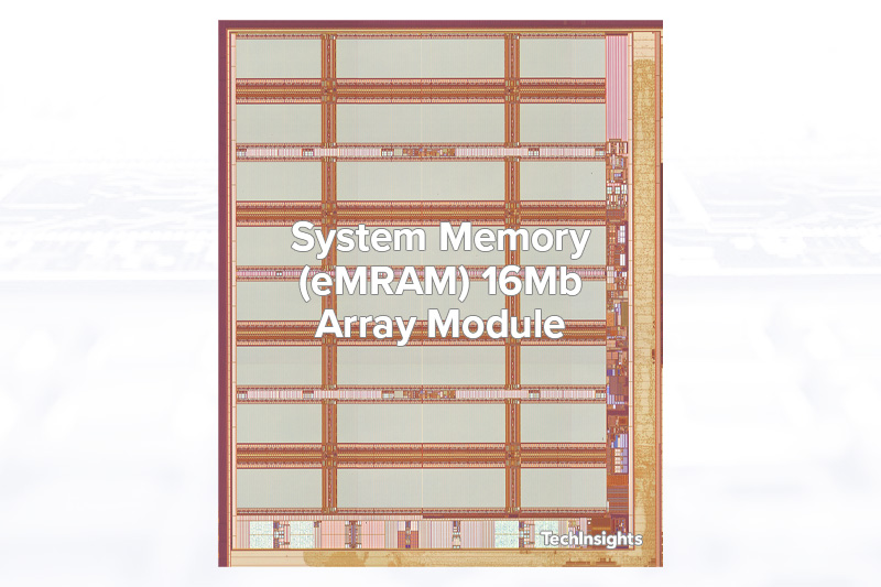
Figure 4. A 16Mb eMRAM array module with TSMC 22ULL process on Ambiq™ Apollo4 Blue MCU die
The Apollo4 MCU employs 2 MB (16 Mb) of MRAM on the 15.56 mm2 MCUdie. Figure 4 shows a 16Mb eMRAM array module with TSMC 22ULL process on Ambiq™ Apollo4 Blue MCU die. Previous Apollo2 (AMAPH) and Apollo3 (AMA3B) SoC products used TSMC 40nm eFLASH process (40ULP) and 2D NOR ESF3 cell structure, the 3rd generation split gate Embedded SuperFlash which consists of EG (Erase Gate), CG (Control Gate), FG (Floating Gate), and WL SG (Select Gate). The low-power eMRAM provides a very large, efficient non-volatile memory for code and data. MRAM doesn’t suffer from the write wear incurred by flash memory.
SEM X-Section and Bevel Top-View Imaging of eMRAM Cell MTJ
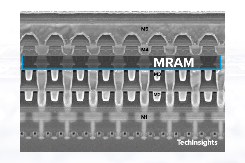
Figure 5. SEM x-section image of TSMC 22ULL eMRAM cell MTJ layer
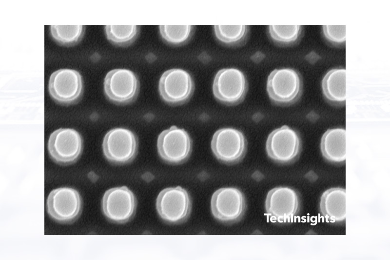
Figure 6. Bevel top-view images of TSMC 22ULL eMRAM cell MTJ layer
Last year, TechInsights did analyses on some recent eMRAM products such as Sony’s GPS SoCs manufactured by Samsung (28 nm FDSOI) and used in Huawei’s smartwatches, as well as Everspin/GlobalFoundries (GF) 28 nm 1 Gb stand-alone DDR4 STT-MRAM and Avalanche/Renesas 40 nm eSTT-MRAM ICs. However, TSMC 22ULL eSTT-MRAM is the most advanced technology node ever to date. The eMRAM 1-bit cell size is 0.046 µm2 which is similar with Everspin/GF’s 28 nm STT-MRAM cell (0.041 µm2). Module area for 2 MB eMRAM on the die measures 1.90 mm2 with sixteen sub-array blocks, and eMRAM sub-array block size is 46,800 µm2 with 220 nm WL pitch and 210 nm BL pitch.
MRAM/MTJ layers are embedded between metal-3 (M3) and metal-4 (M4), circle-typed patterns with 77 ̊etch-angle (x-section). Figures 5 and 6 show the SEM x-section and bevel top-view images of eMRAM cell MTJ layer. In comparison with Apollo3, peripheral and eMemory gate pitches (min.) have been decreased, 170 nm to 120 nm (for peripheral gate), and 230 nm to 110 nm (for eMRAM array) for each.
Ambiq Apollo Blue MCU (microprocessor): Comparative Product Specifications
A comparison of Ambiq™ Apollo Blue MCU series is shown in Table 1 with Apollo2, Apollo3, and Apollo4. Ambiq’s low-power Apollo4 MCUs manufacturing by TSMC on 22ULL process will be comparable with GlobalFoundries’ eMRAM (22 nm FDSOI) which is used for GreenWave’s AI processors, for example. TSMC’s eMRAM is being taken on to 16 nm FinFET platform and will be volume produced in 2022.
| Device | Ambiq™ Apollo2 Blue MCU | Ambiq™ Apollo3 Blue MCU | Ambiq™ Apollo4 Blue MCU |
|---|---|---|---|
| Product Example | Huawei ERS-B29 Band 2 Pro | Huawei TER-B19 Band 3 Pro | Fitbit Luxe (Fitness Band) |
| Package Markings | AMAPH | AMA3B | AMA4B |
| Supply Current | 10 µA/MHz (eFLASH) | 6 µA/MHz (eFLASH) | 3 µA/MHz (eFLASH) |
| Die Markings | Apollo 2 Ambiq Micro 2016 | Apollo 3 Ambiq Micro 2017 | Apollo 4 Ambiq Micro 2020 |
| Die Size (Seal) | 6.43 mm2 (2.55 mm x 2.52 mm) |
10.72 mm2 (3.21 mm x 3.34 mm) |
15.56 mm2 (3.95 mm x 3.94 mm) |
| CMOS Process | 40 ULP | 40 ULP | 20 ULL |
| Foundry | TSMC | TSMC | TSMC |
| Number of Metals | 8 (7 Cu, 1 Al) | 9 (8 Cu, 1 Al) | 10 (9 Cu, 1 Al) |
| Logic Gate Pitch | 170 nm | 170 nm | 120 nm (HKMG) |
| Embedded Memory | eFLASH (2D NOR ESF3) | eFLASH (2D NOR ESF3) | eMRAM |
| eMemory Gate Pitch | 250 nm | 230 nm | 110 nm |
| eMemory Bit Cell Size | 0.068 µm2 | 0.068 µm2 | 0.046 µm2 |
| eMemory Area Portion & Capacity | 14%, 8 Mb | 9%, 8 Mb | 10.4%, 16 Mb |
Table 1. A comparison table of Ambiq™ Apollo Blue MCU series; Apollo2, Apollo3, and Apollo4
Find content like this and more in the TechInsights Platform. Sign-up for free today.
Embedded & Emerging Memory Competitive Insights to Inform your Business Strategy
As the industry has been developing several next generation memory types, technologists are driven to accelerate development and optimize process steps on new device releases. The TechInsights Embedded and Emerging Memory Subscription provides companies with competitive analysis revealing the process design innovations of today’s technology market leaders. Combined with our 30+ years of expertise as well as extensive breadth of analysis and technology, a TechInsights subscription can help inform business strategy by delivering curated, competitive insight on cutting edge technical innovation.
TechInsights Memory offerings have been developed to provide the focused technical intelligence you need based on your industry and role.
![]()


