AMD’s MI300X Takes On H100
Author: Anand Joshi
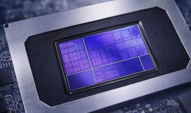
AMD is going after the red-hot data-center AI acceleration market with the introduction of the MI300X accelerator. The MI300X is an enhanced commercial version of the MI300 that was built for the El Capital supercomputer. The accelerator is based on innovative 3D packaging developed by AMD and offers up to 2.6 FP8 PetaOPS at a TDP of 750 W. The accelerator is already in production with AMD’s lead customers that include Meta and Microsoft.
The MI300X is based on AMD’s latest CDNA 3 architecture that unifies the physical memory sharing between CPU and GPU. The MI300X enhances the compute unit to support a range of data formats for AI acceleration, including FP8, integer, brain-float, and tensor-float.
The MI300X integrates up to eight vertically stacked accelerator complex die (XCD) and four IO die (IOD) containing system infrastructure. The die are connected using the AMD Infinity Fabric. The IOD connects to eight high-bandwidth memory (HBM) die, each with 24 GB, via a silicon interposer. The accelerator comes with a 16-lane PCIe 5.0 bus for system connectivity.
AMD has been trying to position its CDNA products as a rival to Nvidia in the data-center AI market. It has had little success so far due to limited AI performance and a weak software stack. AMD has significantly enhanced hardware and software specs in MI300X and expects it to rival Nvidia’s H100. However, there are currently no published benchmarks to compare it apples to apples with the competition.


