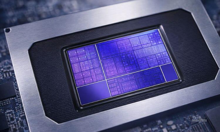
The in-depth image folders will contain the following:
- Downstream product teardown images
- Package X-rays, top metal and poly die photographs, non-invasive optical photos of die features
- SEM bevel through the logic region and NAND flash SEM cross section of the general device structure, BEOL (metals, dielectrics) and FEOL structures
- Two TEM cross sections, orthogonal to the word and bit lines, showing the NAND flash array cells, the lower metals and dielectrics, transistor gates, isolation, and other FEOL feature


