Intel Core Ultra X7 358H Microprocessor: Evaluating the Foveros-S 2.5D packaging technology
The Intel Core Ultra X7 358H brings together three separately manufactured tiles within a single Foveros-S 2.5D package. The processor combines an Intel 18A compute tile with graphics (GPU) and platform controller tiles (PCT) fabricated by TSMC, representing Intel's latest implementation of a disaggregated client microprocessor architecture.
TechInsights has completed an Advanced Packaging Quick Look (APQ) of the Intel Core Ultra X7 358H microprocessor, documenting its package architecture and structural design. The analysis gives engineering teams an independent view of how Intel has implemented its latest client processor package.
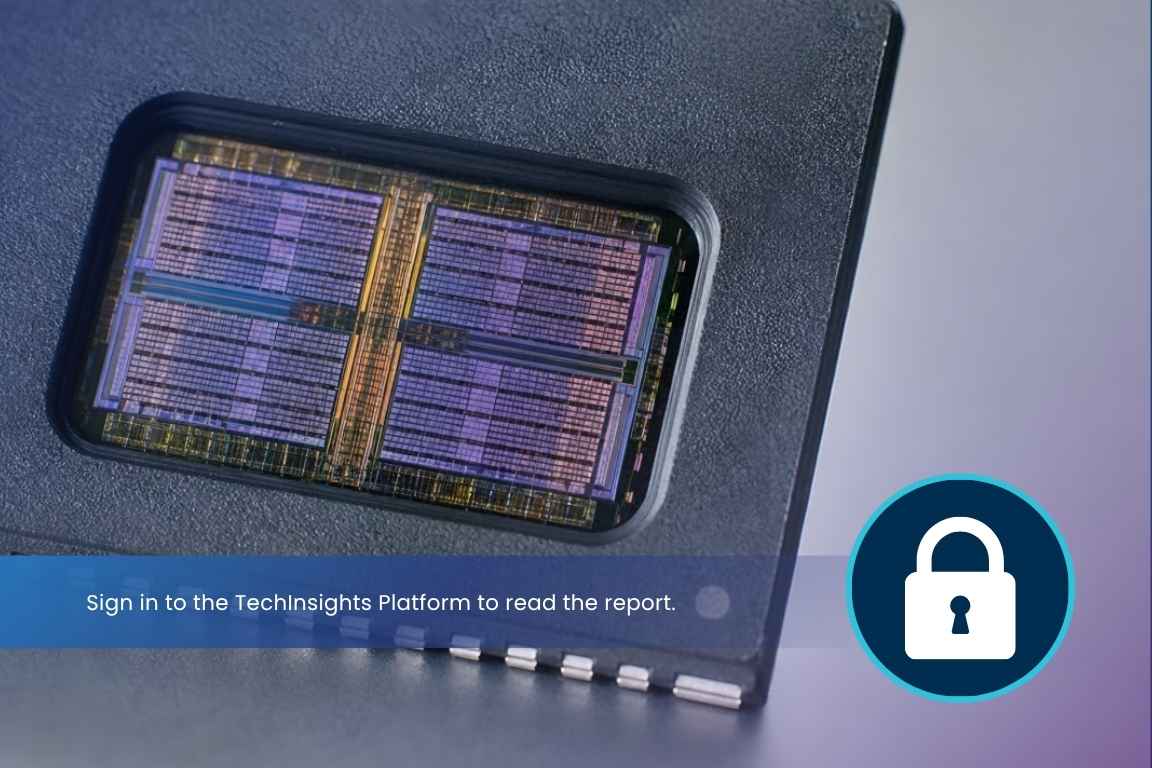
Figure 1 – Evaluating Intel's Foveros-S 2.5D packaging technology (Source: TechInsights)
Intel Integrates Three Process Technologies in One Microprocessor
The compute tile is fabricated on Intel's 18A process node and represents Intel's first high-volume client implementation of RibbonFET gate-all-around transistor technology and PowerVia backside power delivery. It incorporates Cougar Cove performance cores, Darkmont low-power efficiency cores, and an integrated xPU complex. The remaining tiles are manufactured by TSMC, with the GPU using TSMC's 3 nm process. The platform controller tile is fabricated on TSMC's N6 process and consolidates all I/O functionality, such as integrated Wi-Fi on-package wireless solution and Bluetooth connectivity.
The result is a microprocessor that integrates functional blocks fabricated on three different process technologies within a single package.
How Intel Packages the Core Ultra X7 358H
Intel integrates the three active tiles using its Foveros-S 2.5D packaging technology. The compute, graphics, and platform controller tiles are mounted face-down on a passive silicon interposer base tile, which supports power delivery and die-to-die communication.
Communication between the tiles is handled through Scalable Fabric Gen 2. Power is routed from the package substrate through the passive base tile to the active dies. Within the Intel 18A compute tile, PowerVia delivers power through the backside of the die, while an integrated digital linear voltage regulator (DLVR) located close to the transistor loads operates alongside the motherboard voltage regulators.
TechInsights has tracked Intel's packaging technologies across multiple processor generations, including Lakefield, Meteor Lake, Lunar Lake, Granite Rapids, and Sierra Forest. The Intel Core Ultra X7 358H extends that body of analysis with Intel's latest implementation of Foveros-S 2.5D packaging, spanning from early packaging insights through full process and SoC-level analyses.
What's Included in the Advanced Packaging Quick Look Report
The complete Advanced Packaging Quick Look provides a concise analyst summary of the package architecture and critical device metrics, supported by package imagery, structural analysis, and material characterization. The report includes:
- Downstream product teardown
- Package photographs and X-rays
- Die photographs
- Optical planar-view images of selected organic substrate metal layers
- Scanning electron microscopy energy dispersive X-ray spectroscopy (SEM-EDS) analysis of package materials (where observed during preliminary lab work)
- SEM and optical cross-sections of the package structure, dielectric materials, metal layers, dies, and package interconnects
Together, these deliverables document the Intel Core Ultra X7 358H package, from its overall architecture to its materials, interconnects, and structural implementation.