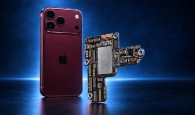
NVIDIA GB10 Superchip (from DGX Spark) Advanced Packaging (Chiplet) Analysis
2 Min Read December 5, 2025
The APC report details NVIDIA's GB10 Superchip, featuring a chiplet design with advanced inter-die communication via NVLink-C2C and Amkor's S-SWIFT.

This Advanced Packaging Essentials - Chiplet (APC) report provides deep insight into the advanced packaging innovations used in the manufacturing of the NVIDIA GB10 Superchip processor, extracted from the NVIDIA DGX Spark desktop computer. The GB10 chip employs a true chiplet, or "dielet", architecture, comprising two separate dies: an "S-Die" that contains the CPU and memory subsystem, and a "G-Die" that contains the Blackwell GPU cores. The two dies communicate via NVIDIA's NVLink-C2C technology, which NVIDIA states delivers 5x the bandwidth of PCIe Gen 5, or up to ~600 GB/s when compared to a PCIe Gen 5 x16 bidirectional configuration. The physical layer providing the C2C inter-die communication is done using Amkor’s Substrate-Silicon Wafer Integrated Fan-Out (S-SWIFT), and marks the first time TechInsights has found use of this packaging technology in a commercially available product.
This summary outlines the analysis* found on the TechInsights' Platform.
*Some analyses may only be available with a paid subscription.