Optimize Semiconductor Costs and Pricing with Confidence
Gain cost transparency, negotiate smarter, and reduce semiconductor spending with industry-leading cost and price models.

Take the Next Step
Ready to see it in action? Enter your information below to schedule a meeting with a TechInsights expert and see how our models can help you drive smarter decisions, reduce costs, and improve your bottom line.
Ready to see it in action?
Book Your Demo!TechInsights' Semiconductor Manufacturing Economics models provide procurement professionals with in-depth, bottom-up cost simulations of the entire semiconductor production process – from wafer fabrication to assembly and test – giving you quantitative insights into prices and cost categories, including equipment, materials, facilities, and labor. Learn about TechInsights’ comprehensive portfolio of semiconductor cost and price modeling tools included within Semiconductor Manufacturing Economics.
Unlock Cost Transparency and Pricing Power:
- Negotiate smarter: Leverage detailed insights into semiconductor manufacturing costs
- Lower costs: Reduce purchasing prices with insights into semiconductor manufacturing costs based on product volumes
- Make informed decisions: Quantify the cost difference of a larger or more complex die
- Gain market advantage: Stay ahead with projections from 2015 to 2035, covering a wide range of technologies
Use Cases
How It Works: The Cost and Price Modeling Process
![]()
Step 1
Model semiconductor manufacturing costs using verified industry or TechInsights reverse engineering data
![]()
Step 2
Compare against supplier quotes or internal cost structures
![]()
Step 3
Identify margin discrepancies, cost reduction opportunities, and pricing benchmarks
![]()
Step 4
Negotiate effectively using fact-based data

Who Uses These Models?
For Procurement and Supply Chain Teams: Conduct should-cost analysis to negotiate pricing
For Foundries and IDMs: Benchmark fab costs and optimize operational efficiency
For Materials and Equipment Suppliers: Check foundry price requests and defend fair supplier pricing

Why Trust TechInsights:
Industry-Leading Expertise: 24+ years of semiconductor cost modeling experience
Trusted by Top Semiconductor Manufacturers: Used by leading Fabs, IDMs, Foundries, and Capital Equipment Manufacturers.
Data-Backed Insights: Our Cost models are validated against real-world production data.
Model Information

Assembly and Test Cost and Price Model
Easily estimate manufacturing costs and selling prices for most IC testing and assembly operations and also get total product cost using wafer cost inputs.
It includes:
- Cost and price for assembly and test of semiconductors
- Unit cost and price, materials requirements, and equipment requirements
- Cost and price by process, volume, and date from 2010 to 2035

Discrete and Power Products Cost and Price Model
Seamlessly estimate the cost and selling price of high-power silicon and compound semiconductor integrated circuits and discrete devices.
It includes:
- Wafer fabrication, test, and packaging costs
- Coverage of 100mm to 300mm wafer sizes
- Cost (manufacturing cost) and price (selling price) estimates for a wide range of semiconductors
- Cost and price by volume and date from 2015 to 2030

IC Cost and Price Model
Easily estimate the cost and selling price of low-power silicon integrated circuits.
It includes:
- Wafer fabrication, test, and packaging costs
- Coverage from 3-µm technologies on 100mm wafers to the latest in production state-of-the-art on 300mm wafers
- Cost (manufacturing cost) and price (selling price) estimates for a wide range of semiconductors
- Cost and price by volume and date from 2015 to 2030

Strategic Cost and Price Model
Explore past, current, and future technologies from the leading producers in four segments: DRAM, Foundry and IDM Logic, and NAND. The model is a wafer cost and price model only and produces detailed wafer costs, equipment sets, and materials.
It includes:
- Cost and price for leading-edge 300mm wafer processes
- A detailed technology roadmap for 3D NAND, DRAM and Logic, and equipment and materials requirements
- Cost and price by process, volume, and date from 2000 to 2035

Fab Database
Get access to the world’s most detailed database of global semiconductor fabs.
It includes:
- 300mm Watch database contains all 300mm wafer fabs both current and planned, including locations, key dates, partners, capital investments, incentives, nodes, products, capacities (from 2010 to 2030), and analysis graphs
- Semico Fab database of >1000 operating, planned, and closed global semiconductor fabs from 3-inch to 300mm, including locations, key dates, capital investments, nodes, products, capacities (from 2018 to 2023) and analysis graphs

Inside Smartwatch Costs: Xiaomi, Samsung, and Huawei Compared
TechInsights compares the Xiaomi Watch 5, Huawei Watch GT 5 Pro, Samsung Galaxy Watch8 LTE, and Xiaomi Watch S4, revealing how processors, LTE connectivity, displays, and batteries drive smartwatch BOM costs.

Meta Ray-Ban Display Teardown Reveals More Than Meets the Eye
TechInsights analyzes the Meta Ray-Ban Display and Neural Band, uncovering Qualcomm AR1, display cost drivers, Sony imaging, and key design wins.
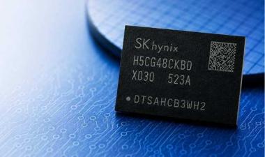
SK hynix D1c DRAM Analysis: EUV Drives HBM4E and HBM5
TechInsights analyzes SK hynix's D1c DRAM node, revealing its mature EUV strategy and implications for HBM4E, HBM5, DDR5, and AI memory.
![]()
The Authoritative Information Platform to the Semiconductor Industry.

