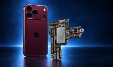
HiSilicon Kirin 9030 Pro Process Flow Analysis
How Does SMIC’s N+3 Process Compare to Leading-Edge Nodes?
TechInsights has reverse-engineered the process flow of the HiSilicon Kirin 9030 Pro, fabricated by SMIC using its N+3 process technology. The analysis examines front-end-of-line (FEOL) and back-end-of-line (BEOL) critical dimensions, patterning strategies, and the complete lithography mask set.
The work addresses a question facing semiconductor process engineers, chip designers, competitive intelligence teams, and technology strategists: How does SMIC’s N+3 process compare with leading-edge nodes from TSMC and Samsung? Answering that question requires measured, layer-by-layer evidence. Fin pitch, gate pitch, metal pitches across the interconnect stack, via dimensions, and the lithography technologies used at each layer all help establish how SMIC implemented N+3. These details provide a technical basis for evaluating patterning complexity, metal stack architecture, and lithography tooling.
The analysis is particularly relevant given the continued attention on SMIC’s domestic advanced logic capabilities and its role in supplying leading Chinese chip designers under ongoing export controls. Its findings can inform competitive benchmarking, equipment procurement planning, and assessments of China’s progress toward greater self-sufficiency in advanced logic fabrication.
Figure 1 – HiSilicon Kirin 9030 Pro Process Flow Analysis (Source: TechInsights)
Earlier Kirin 9030 Analysis Confirmed SMIC N+3
TechInsights previously conducted an exploratory teardown and process analysis of the Kirin 9030 application processor used in the Huawei Mate 80 Pro Max. At the time, industry observers had questioned whether Huawei’s latest flagship processor used a 5nm process, a 6nm process, or an enhanced version of SMIC N+2. SMIC had not published a roadmap identifying those nodes, making physical analysis of the processor an important source of evidence about the foundry’s manufacturing capabilities.
TechInsights’ structural and dimensional measurements confirmed that the Kirin 9030 was manufactured using SMIC N+3. The analysis identified it as a scaled evolution of SMIC’s 7nm-class process and examined how far the foundry had advanced toward a 5nm-equivalent process without extreme ultraviolet lithography.
The earlier comparison found meaningful density improvements beyond SMIC N+2. It also established that the SMIC N+3 remained significantly less scaled than the commercial 5nm processes offered by TSMC and Samsung. That work established which process SMIC used. The new process flow analysis examines how SMIC implemented it.
Ask Insightful Chat about this device - Instant insights powered by AI trained on comprehensive semiconductor data.
How the Kirin 9030 Pro Process Flow Analysis Examines SMIC N+3
The new analysis extends the investigation through a detailed reconstruction of the SMIC N+3 process flow. It measures the structures and critical dimensions that define the process across both the transistor and interconnect levels. The FEOL analysis covers measurements such as fin pitch and gate pitch. The BEOL analysis tracks metal pitches across every interconnect level, along with via dimensions and the architecture of the metal stack. The complete lithography mask set documents the patterning technologies used at each layer.
Together, these findings provide the evidence needed to compare SMIC N+3 with leading-edge processes from TSMC and Samsung. They also help clarify where SMIC has scaled beyond its earlier 7nm-class technology, how much patterning complexity the process requires, and what it reveals about the limits of deep ultraviolet (DUV) manufacturing.
Create your Account Today
Access the complete HiSilicon Kirin 9030 Pro Process Flow Analysis, including the measured process dimensions, patterning strategies, metal stack details, and lithography mask set.
*Some analyses may only be available with a paid subscription