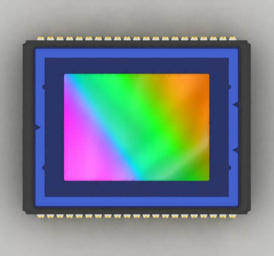
CMOS Image Sensor Architecture, Pixel Design, and Stacked Image Sensors
Decode Competitive Image Sensor Design
See exactly how leading semiconductor brands design competitive CMOS image sensors. This analysis reveals how pixel architecture, stacked image sensor integration, and process technology choices move from concept to high-volume production—and which innovations actually deliver real-world imaging performance.
Frequently Asked Questions (FAQs)
- What is image sensor design?
-
Image sensor design encompasses pixel architecture, stacked sensor integration, readout circuitry, and manufacturing process choices that determine imaging performance, power, cost, and scalability.
- What types of image sensors are covered?
-
This analysis focuses on CMOS image sensors, including advanced pixel designs and stacked CMOS image sensor architectures used in production devices.
- Is this analysis vendor-specific?
-
No. The decode examines competitive image sensor design approaches across leading semiconductor companies, highlighting common patterns and differentiators.
- How is this different from academic or vendor papers?
-
This analysis is based on real CMOS image sensor teardown data, revealing what was actually built and shipped rather than proposed or marketed.
- Does this cover production-ready image sensor technology?
-
Yes. A core objective is to identify image sensor innovations that made it into high-volume production and delivered real-world performance.
- Is this image sensor analysis available now?
-
Yes. Decode Competitive Image Sensor Design is available now through TechInsights.