Industry-Leading Reverse Engineering
From Physical Device to System-level Insight
TechInsights provides industry-leading reverse engineering services for semiconductor and electronic systems, delivering detailed technical analysis from physical device teardown to system-level architecture.
1.7M+
100K+
650+
35+
Process Reverse Engineering
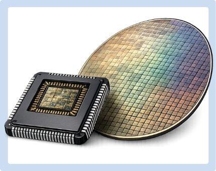
TechInsights perform step-by-step process flow reconstruction based on physical device analysis — revealing the sequence of lithography, deposition, etching, and integration steps used in wafer fabrication and advanced packaging. This insight enables you to understand manufacturing strategies at a fundamental level.
Decode the Process. Discover the Strategy.
Circuit Extraction
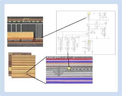
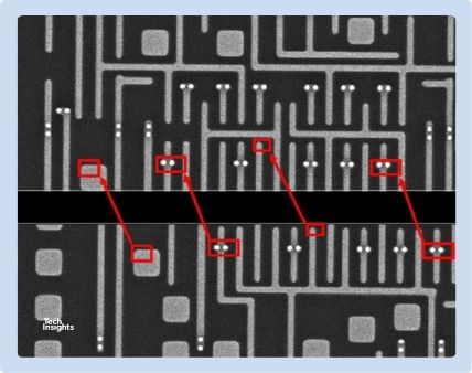
Our experts extract die-level circuit layouts, functional blocks, transistor structures, and interconnect architectures from devices using state-of-the-art imaging, SEM/TEM analysis, and schematic reconstruction tools. This capability powers deep circuit visibility for design optimization and competitive intelligence.
Circuit Insight That Drives Competitive Edge.
System Reverse Engineering
Take advantage of full system-level deconstruction including SoC floorplan analysis, functional block organization, and architectural innovation assessment. We uncover how subsystems interact, how data flows, and where key performance differentiation originates.
Architecture Exposed. Advantage Explained.
Performance Testing and Characterization
TechInsights goes beyond structural analysis — we conduct performance testing, reliability assessment, and operational analysis under varied conditions to evaluate how real devices function in practice, providing actionable performance intelligence.
Performance Proven. Not Assumed.
Advanced Teardowns & Materials Analysis
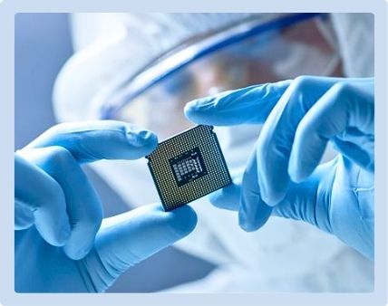
From semiconductor chip teardowns to advanced packaging and MEMS, our multidisciplinary teams reveal design strategies, material use, and architectural choices across a broad array of technologies.
Deconstructing Innovation, Layer by Layer.
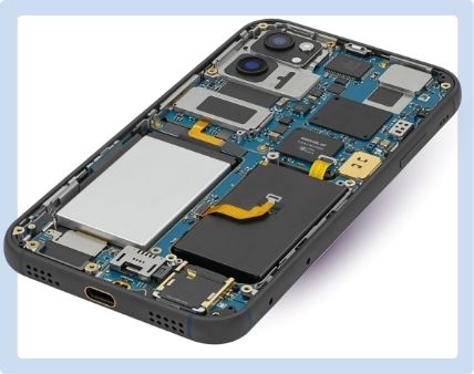
Why Leading Organizations Trust TechInsights Reverse Engineering
TechInsights delivers unmatched technical visibility into today’s most advanced semiconductor and system designs. Using industry-leading tools and deep domain expertise, we expose hidden innovation across logic, memory, RF, power, sensor and High Performance Computing (HPC) technologies—transforming complex silicon and systems into clear, actionable intelligence.
Our reverse engineering extends beyond inspection. High-fidelity visual and schematic analysis fuels competitive benchmarking, market intelligence, and patent workflows—supporting confident roadmap, investment, and product decisions. From evidence-of-use to infringement evaluation, TechInsights provides trusted technical proof when accuracy matters most.
Unmatched Technical Visibility
Expose hidden innovation at every layer—from device physics to system architecture.
Competitive Benchmarking & Market Intelligence
Compare designs, track technology trends, and inform strategic decisions with confidence.
Patent & IP Evidence Support
High-fidelity imagery and schematics to support validity, infringement, and EoU strategies.
Drive Innovation & Reduce Risk
Turn deep technical insight into faster R&D, smarter design choices, and stronger IP positions.
High Performance Computing Benchmarking
Independent lab validation of HPC systems at the server node and accelerator card-level, delivering vendor-neutral performance, power, thermal, and energy-to-solution insights beyond vendor telemetry for competitive benchmarking and procurement decisions.
Frequently Asked Questions

Apple A20 Pro: Inside the iPhone 18 Pro’s TSMC 2nm Processor
TechInsights analyzes Apple’s A20 Pro processor, revealing TSMC N2 gate-all-around technology, expanded AI and graphics processing, and a new side-by-side memory packaging architecture.

iPhone 18 Pro Max Unboxing and First Look
Watch TechInsights unbox the Apple iPhone 18 Pro Max before our experts begin detailed teardown and semiconductor analysis.
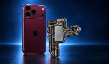
Apple iPhone 18 Pro Max Teardown: A20 Pro, X80 and Apple N1
See what TechInsights’ preliminary teardown reveals about the iPhone 18 Pro Max, including its A20 Pro processor, Qualcomm X80 modem, Apple N1, and new mmWave hardware.

The Authoritative Information Platform to the Semiconductor Industry.