Welcome to the TechInsights Platform.
Your free account is confirmed. You now have access to advanced-packaging analysis, teardown highlights, and Insightful Chat.
The shift to chiplets, HBM, 2.5D and 3D stacking is changing how the industry builds compute. Inside the Platform, you can explore the packaging technologies behind today’s leading AI accelerators, HPC designs, and flagship SoCs.
Sign in with the corporate email address you used to register.


Have a question? Ask it now.
Have a question about chiplets, HBM, advanced packaging, or heterogeneous integration? Open Insightful Chat and ask it now.
Try it, you already have access.
Continue exploring
Go deeper into the Platform to find the analysis behind the industry's most important packaging decisions.

Apple A20 Pro: Inside the iPhone 18 Pro’s TSMC 2nm Processor
TechInsights analyzes Apple’s A20 Pro processor, revealing TSMC N2 gate-all-around technology, expanded AI and graphics processing, and a new side-by-side memory packaging architecture.

iPhone 18 Pro Max Unboxing and First Look
Watch TechInsights unbox the Apple iPhone 18 Pro Max before our experts begin detailed teardown and semiconductor analysis.
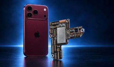
Apple iPhone 18 Pro Max Teardown: A20 Pro, X80 and Apple N1
See what TechInsights’ preliminary teardown reveals about the iPhone 18 Pro Max, including its A20 Pro processor, Qualcomm X80 modem, Apple N1, and new mmWave hardware.

The Authoritative Information Platform to the Semiconductor Industry.