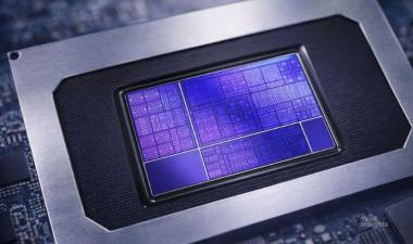
SmartSens SC100AT Standard Floorplan Analysis

Explore the in-depth analysis of the SmartSens SC100AT image sensor die, featuring 1.3 MP resolution and a 3.0 µm pixel pitch for automotive applications. This report includes foundry identification, key features, SEM cross-sections of periphery circuits, die functional floorplan, and cost details.
Insight into the structure of the SmartSens SC100AT image sensor die, which is a 1.3 MP resolution, monolithic (BI) CIS with a pixel pitch of 3.0 µm for automotive applications, particularly on its periphery circuitry. The analysis provides foundry identification, and a summary of the salient features observed that is accompanied by a set of SEM cross-section of the image sensor periphery circuits. The die functional floorplan and cost information are also included in the report.


