Posted: April 11, 2014
Contributing Authors: M. Alarcon, R. Fontaine, D. James, R. Krishnamurthy, J. Morrison, D. Yang and C. Young
Samsung Galaxy S5
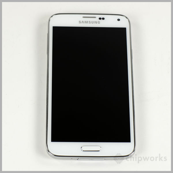
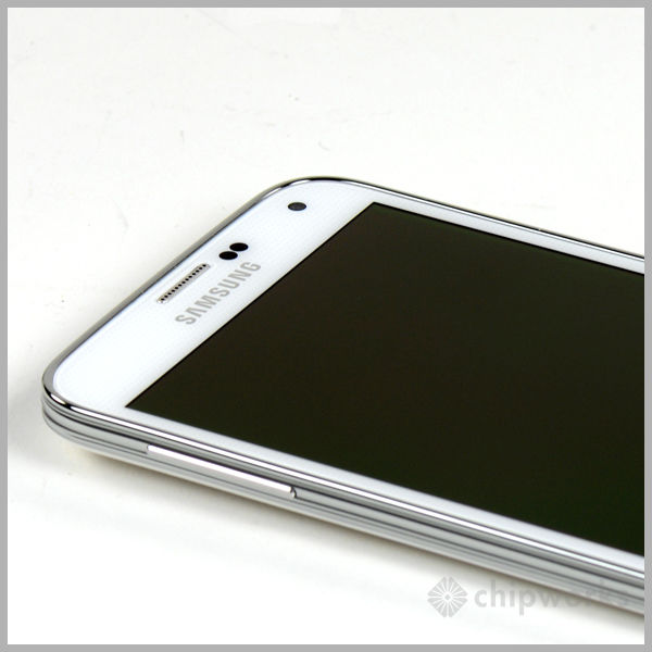
Samsung unveiled their Galaxy S5 in Barcelona during this year’s Mobile World Congress. Although Samsung’s official global launch wasn't until later in April, we managed to get our hands on one earlier than most folks. The 5.1 inch multi-band phone comes equipped with a quad-core, 2.5GHz processor with 2GB of RAM and a 16 MP camera. Since we have seen differences from region to region with Samsung phones, it is worth pointing out that this particular SM-G900S phone was sourced in South Korea.
As competition intensifies from rivals such as HTC, Huawei, Xiaomi and other Chinese phone makers, our teardown analysis provides a technical look at how Samsung attempted to differentiate itself. See below as we have set to unveil new innovations and design wins inside the Samsung Galaxy S5.
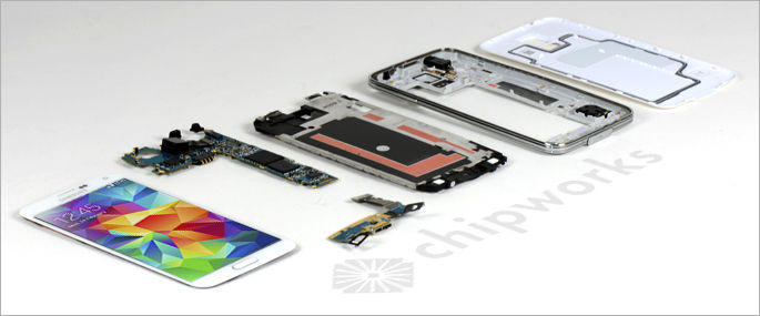
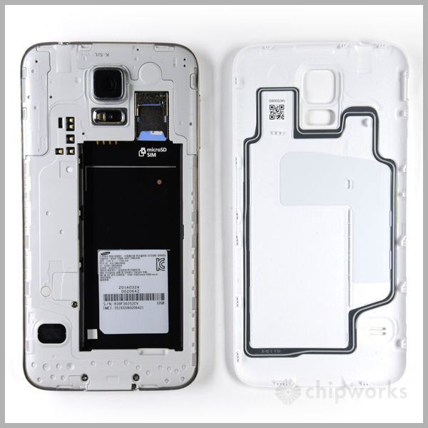
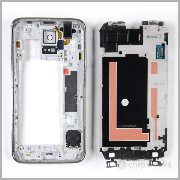
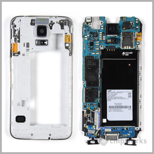
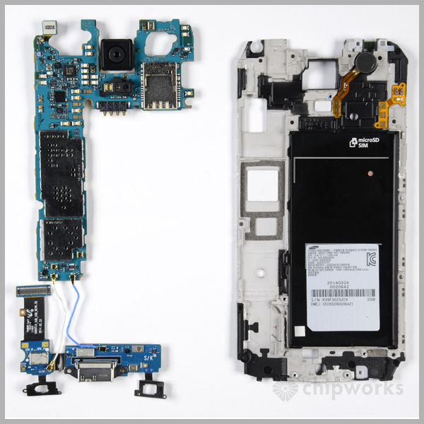
Inside the S5
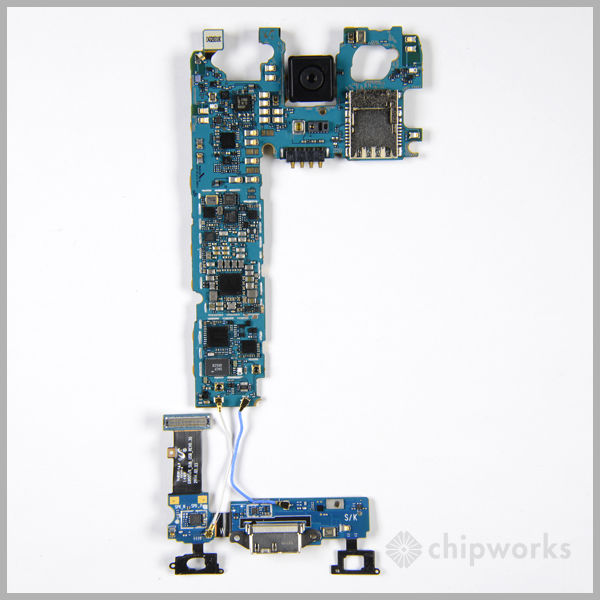
A look inside the S5
Although we’ve already seen many devices inside the Samsung Galaxy S5, our engineers are pretty interested in 3 big pieces of innovation. First is the phone’s new 16 MP, 1/2.6” optical format primary camera module. Second is the world’s first dedicated heart rate monitor also known as a Biosensor - Pulse/Oxy IC. Third is the fingerprint scanner. The latter is a particularly interesting story as it is not designed like the iPhone 5S’ circular home button but instead integrates the touch screen into its operation, more on that below.
Design Wins
Design Wins
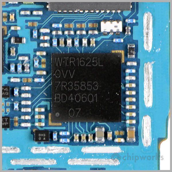
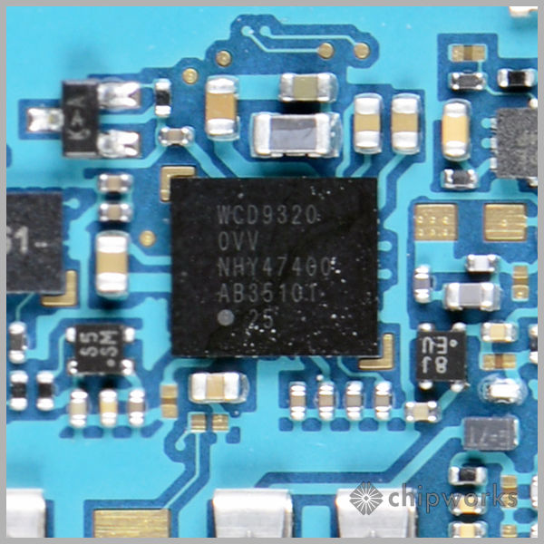
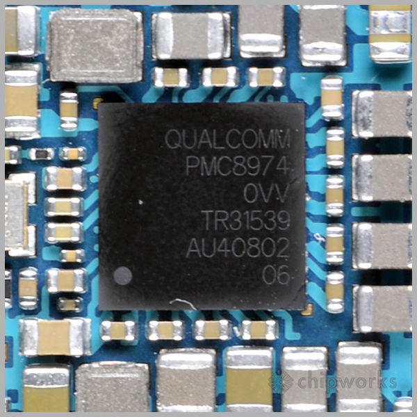
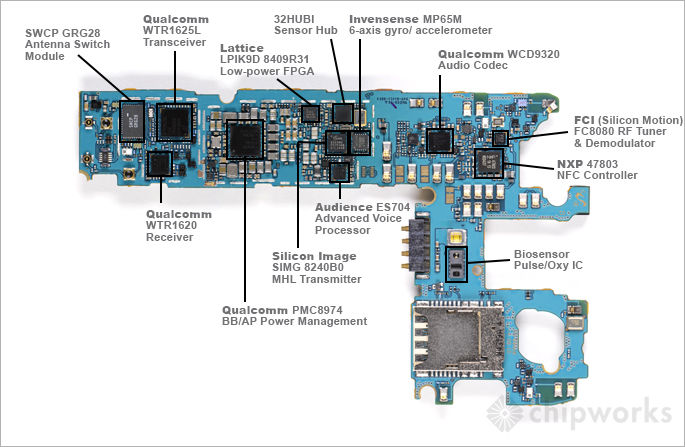
We’ve been able to identify multiple chips inside the Galaxy S5. Qualcomm appears to have the most socket wins with:
- QFE1100 (Envelope Tracking Power Amplifier PMIC),
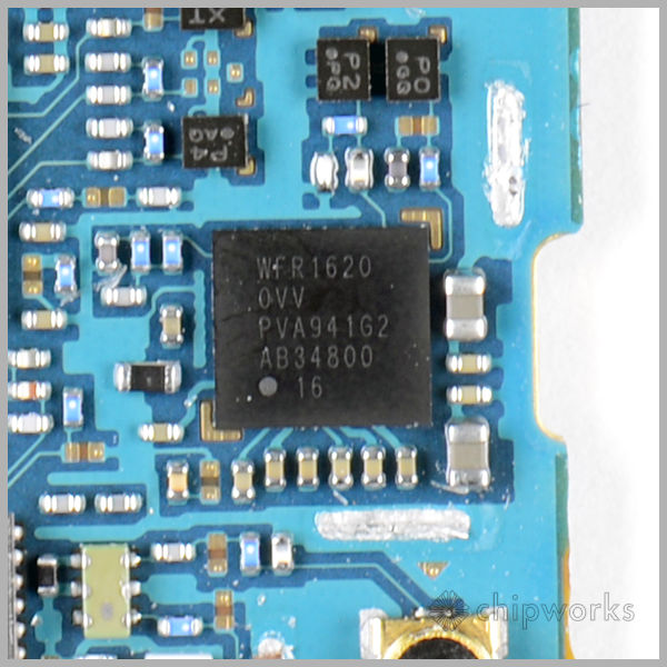
- WFR1620 (RF Receiver),
- WTR1625L (RF Transceiver),
- MSM8974AC (Snapdragon 801 (BB/AP SoC)),
- WCD9320 (Audio Codec) and
- PMC8974 (BB/AP Power Management).
Other notable chips include:
- Avago A7007 (Band 7 PAM),
- Avago ACPM-7617 (MMMB 2G/Edge, 3G, LTE) and
- Avago +ACW (FBAR)
- Maxim MAX77804K (System PSoC) and
- Maxim MAX77826 (likely Battery/Power).
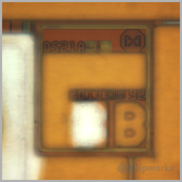
- Rumors alleged that Maxim won the Biosensor socket but initially package marks did not validate this. Further analysis says it is in fact Maxim (OS21A).
- Audience’s ADNC ES704 (Stand-alone voice processor),
- FCI’s FCI FC8080 (Terrestrial Digital Multimedia Broadcast RF Tuner & Demod),
- Invensense’s MP65M P02881 L1405 (6-axis gyro/accelerometer),
- Lattice’s LP1K9D (Low-power FPGA),
- NXP’s NXP 47803 (NFC + Secure Element (Region specific)),
- RFMD’s RF1119 (Antenna Control Solution),
- Samsung’s own K3QF2F0DA (Likely 2GB RAM),
- KLMBG4GEAC (32 GB flash), and
- Silicon Image’s SIMG 8240B0 (MHL Transmitter)
- Audience eS704 (Audio CODEC)
- FCI FC8080 (Demodulator)
Unidentified Silicon
Unidentified Silicon
Unidentified Silicon
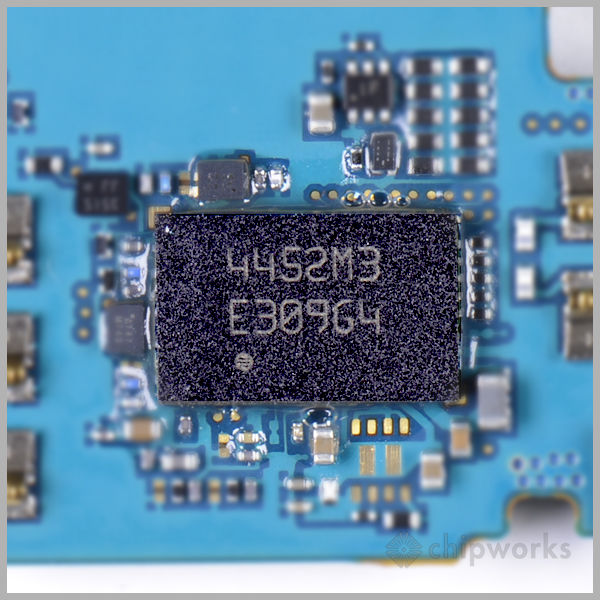
A chip with the package markings “32HUBI A5006V0 W 404 A” is likely the sensor hub and we think it is possibly manufactured by STMicro, but we cannot confirm any of this yet. We also found a chip with the package markings “4452M3” likely manufactured by Semco or STMicro (no confirmation yet), this chip serves as the WLAN Module and we think Broadcom’s BCM4354 is inside that package.
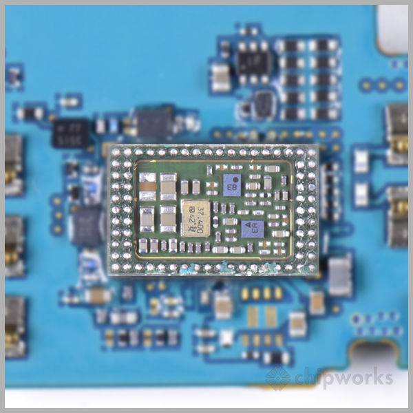
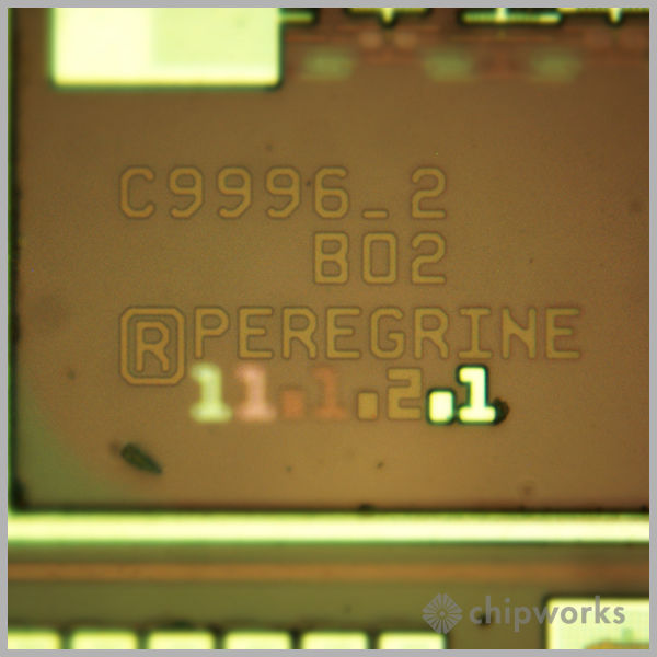
Antenna Switch Module
Antenna Switch Module
This module is the FEMiD, Front End Module with Integrated Duplexers from the Galaxy S 5. Inside is the Peregrine RF CMOS antenna switch. This device is a double pole, fourteen throw switch (DP14T). The switch goes by Peregrine part number PE421281. Peregrine has been observed by us in 16 unique multiband handsets recently; From iPhones and cellular enabled iPads to Samsung Galaxys. This a very high volume part for Peregrine, big win for the US-based RFIC fabless provider.
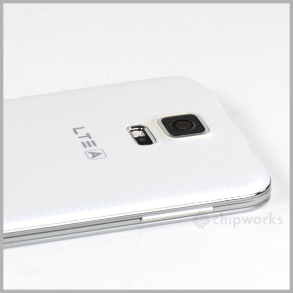
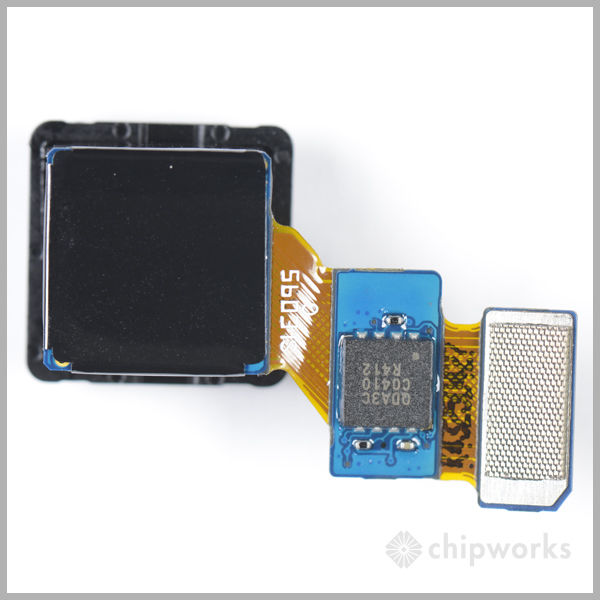
Galaxy S5 Cameras
Galaxy S5 Cameras
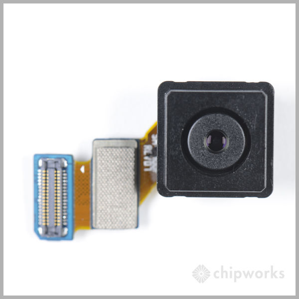
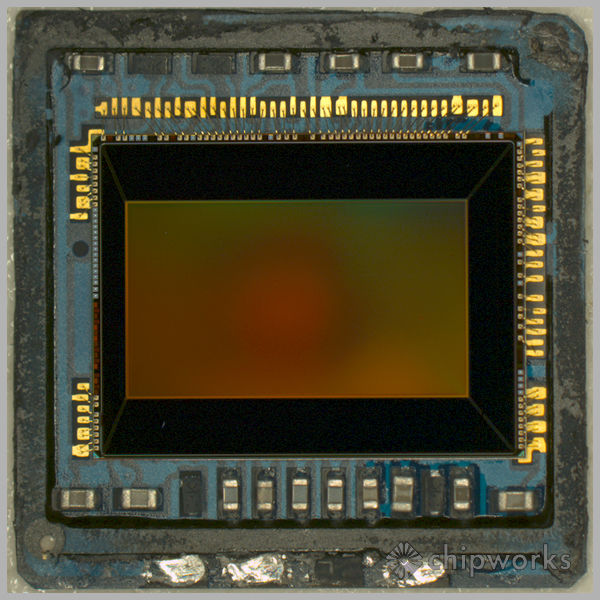
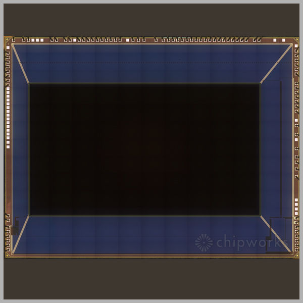
One of the biggest stories of the Galaxy S5 is the new 16 MP, 1/2.6” optical format primary camera module. Going back to the Galaxy S II we found back-illuminated Samsung and Sony 8 MP, 1/3.2” optical format CMOS image sensor chips in S II phones from different regions. All the Galaxy S III phones we analyzed used 8 MP Sony camera chips, suggesting the Sony team captured all the business for the third iteration of Samsung’s marquee smartphone. This apparent trend continued on to the Galaxy S4 and Note 3, which used the popular 13 MP Sony IMX135 featuring Sony’s stacked chip (Exmor-RS) technology.
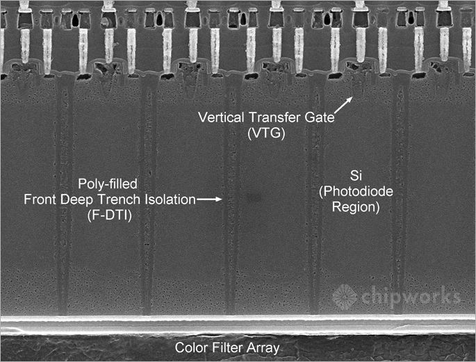
Not to be outdone, the Samsung image sensor team developed its ISOCELL technology. Announced in September, 2013 [1] ISOCELL reportedly enables a 30% reduction in crosstalk and 30% increase in full well capacity. Samsung described ISOCELL technology in a February webinar and again at Image Sensors 2014, promoting it as the next key image sensor technology after back-illuminated (BSI) sensor technology. The salient points include: the successful implementation of front deep trench isolation (F-DTI) and vertical transfer gates (VTG). We found both of these technology elements in 2013 from other companies: F-DTI from STMicroelectronics in its HTC ONE UltraPixel camera chip, and VTGs from Sony in a Cyber-shot camera [2]. Below is a cross-section of an 8 MP version of Samsung’s ISOCELL technology showing the F-DTI and VTG. For clarity: this is not from the Galaxy S5, but we expect to uncover the same fundamental structures as we dive in to our 16 MP ISOCELL analysis. We also expect to find phase detection autofocus (AF) pixels and will update our teardown when we have more details.
Samsung CIS
The Samsung CIS group isn’t stopping there. It announced a stacked chip image sensor in February at Mobile World Congress [3]. While Samsung hasn't been first to market with new technology elements such as BSI, per-pixel DTI, VTG pixel transistors, or stacked chip, it continues to successfully bring these technologies into mass production. What will we find in upcoming Samsung flagship phones? Time will tell, however it appears that at this moment in time Samsung can go toe-to-toe with Sony and win.
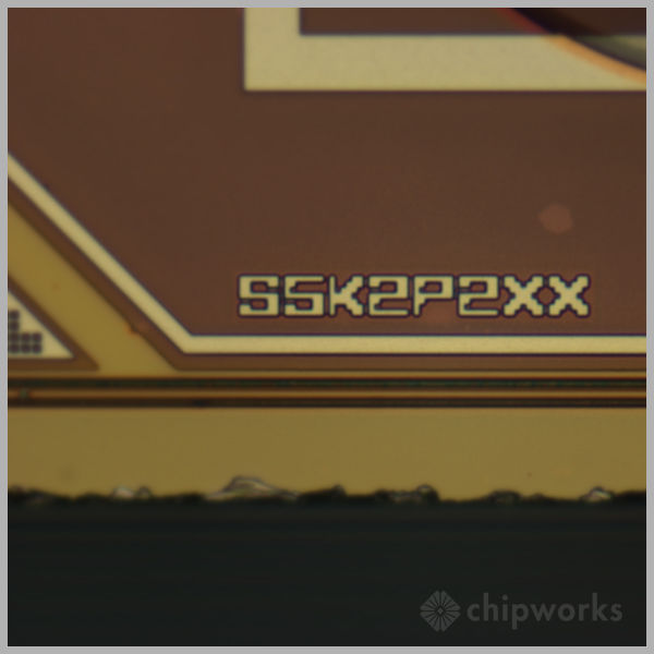
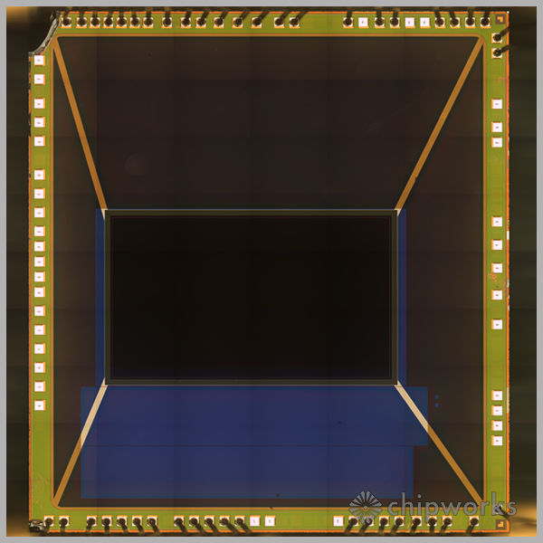
We’ve removed the 16 MP ISOCELL primary and 2.0 MP secondary camera chips from the respective camera modules and found two back-illuminated Samsung CMOS image sensors. The primary camera chip, having S5K2P2XX die markings, features a 1.12 µm pixel pitch. Phase-detection pixel pairs are distributed across nearly the entire active pixel array. This marks the smallest phase detection pixel generation we’ve seen and only the second time we’ve seen them on a back-illuminated chip (Toshiba was first @ 1.4 µm). The presence of phase detection pixels also implies the use of a back aperture grid (with the phase detection pixels being half-masked). The use of an aperture grid would also be a first for Samsung (based on our analysis) and we’ll be covering this and the other technology elements in our planned full report.
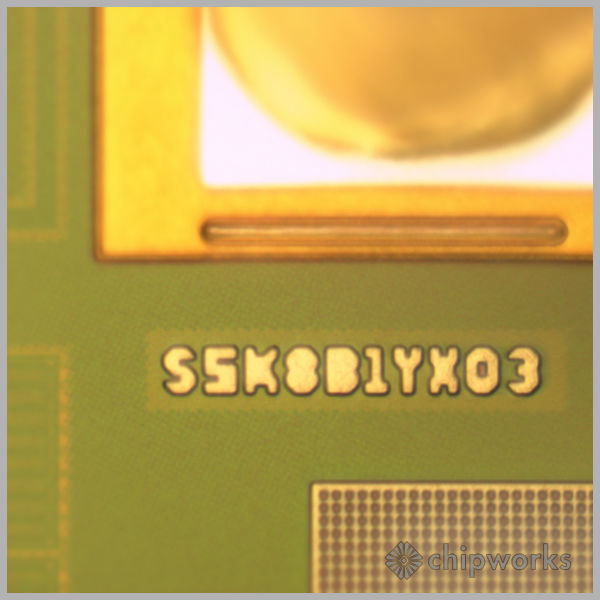
The back-illuminated secondary camera chip, having S5K8B1YX03 die markings, has a 1.12 µm pixel size.
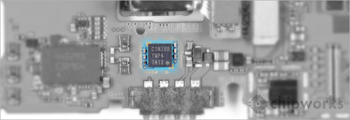
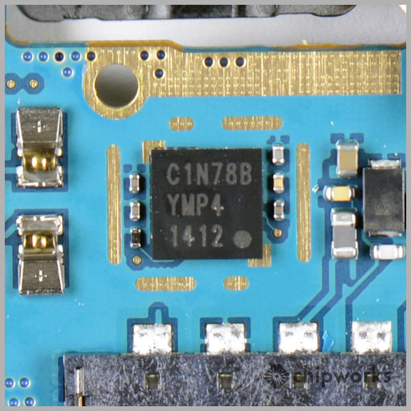
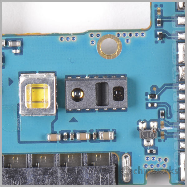
Heart Rate Monitor
The Dedicated Heart Rate Monitor aka Pulse Oximeter
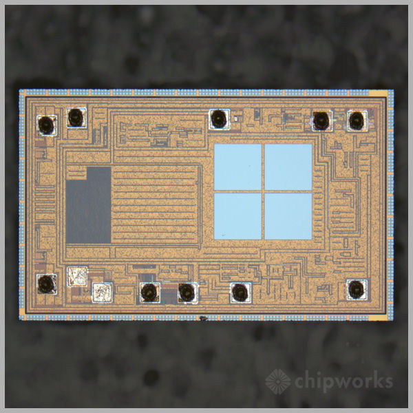
The heart rate monitor is next to the LED camera flash on the back of the phone - it works by illuminating your finger with red/infra-red light, and monitoring the changing reflection as your finger pulses with your heartbeat. Some set-up is required to define a baseline, but after that it seems to work fine (at least according to the video reviews). We had several inquiries as to who can claim to have won the pulse socket. We were not sure as there were no package markings on the device. All that was visible were the emitter and the detector. Our lab went to work last Friday on the module and we were very surprised to see a CSP device from Maxim. The Maxim web site speaks to Pulse Oximeter solutions and the die mark on this device carries Maxim die marks. That is 3 devices so far for Maxim inside this GS5 model.
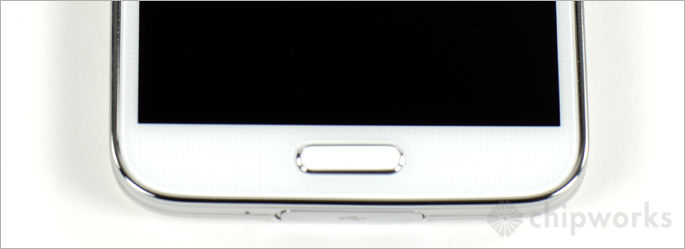
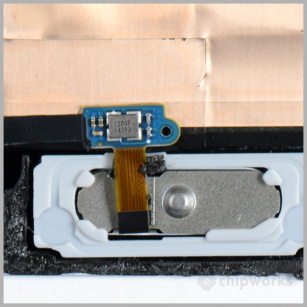
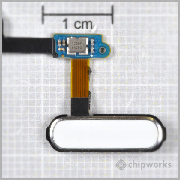
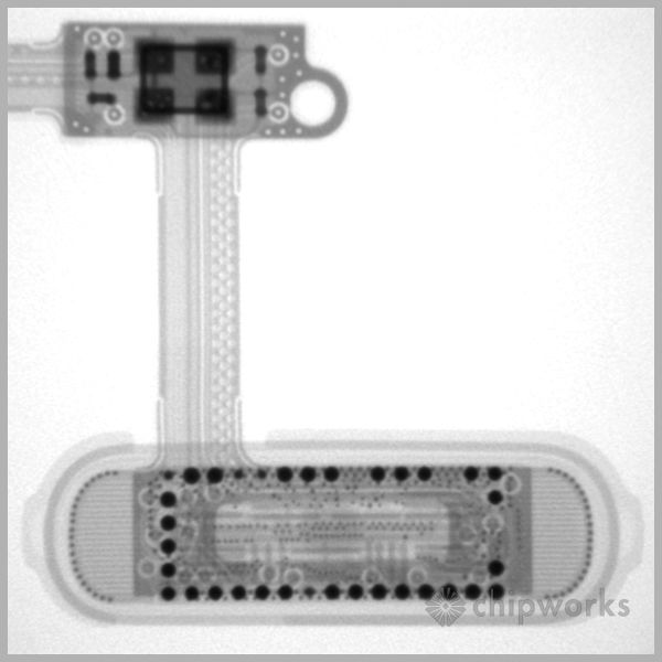
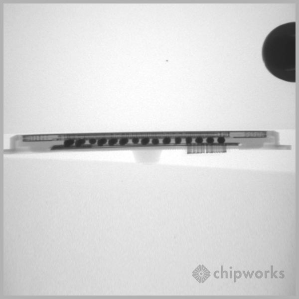
The Fingerprint Sensor
The Fingerprint Sensor
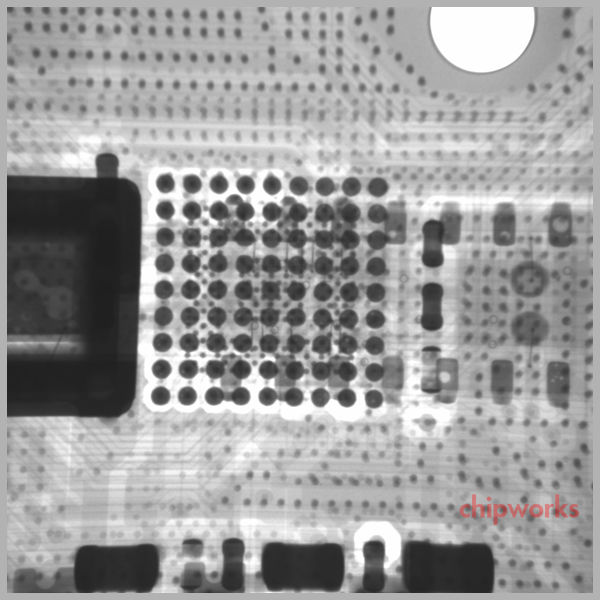
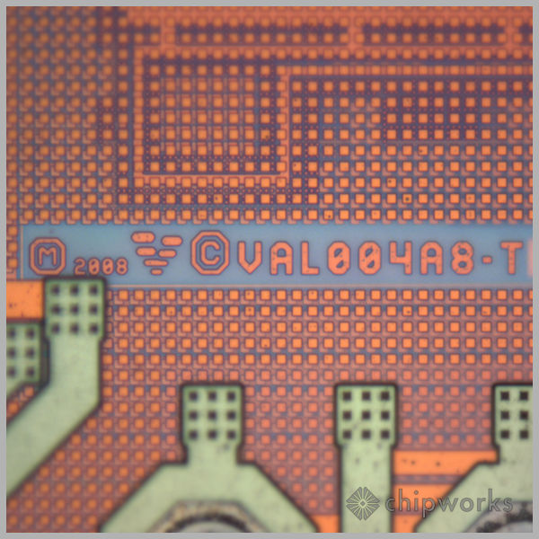
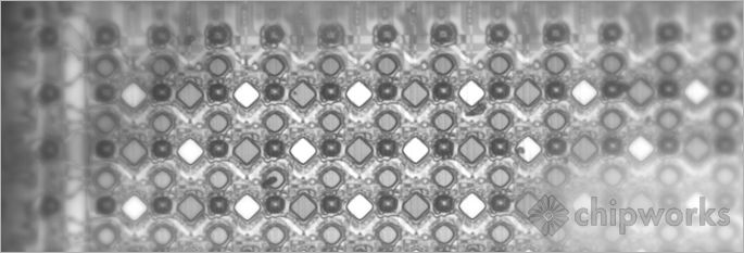
The fingerprint sensor, as we noted earlier, is a different beast from the one in the iPhone. It seems to be split into two parts - a touch sensor incorporated into the home button, but it also takes input from the main touch screen, and both have to be used to get your ID loaded. The technology behind this fingerprint sensor is hidden behind the home button. The button in question is really a fingerprint scanner from Synaptics (Validity Inc acquired by Synaptics in Q4 2013). Embedded in the home button is a Chip-on-Flex module that scans your swirls and whorls and validates that you are who you say you are. We’ve added new x-ray and infrared images below. There is clearly an IC in there. Given the involvement of the touch screen, the Synaptics controller, and the acquisition of Validity, it is tempting to conclude that Samsung is using the Synaptics “Natural ID” fingerprint ID technology.
Our latest image (last image below) from the lab is what we like to call the smoking gun! Check out the Synaptic die mark! We will see from images obtained through further de-processing, that this “home button” is really a great example of “what’s inside technology”. Our engineers are all wondering how this two step fingerprint ID works?!
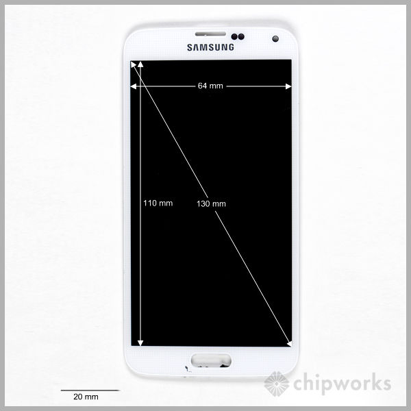
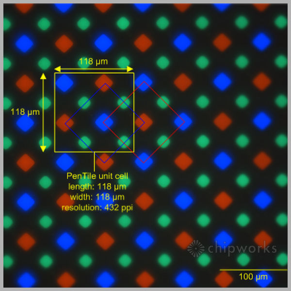
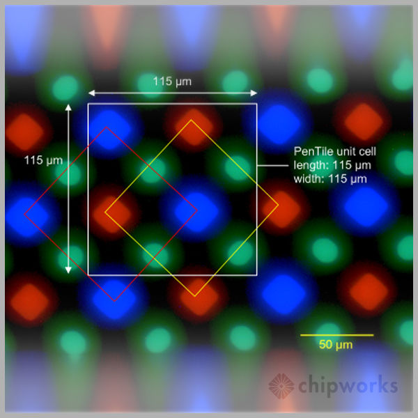
The Full HD Super AMOLED Display
The Full HD Super AMOLED Display
The Samsung Galaxy S5 full HD super AMOLED display, just like its predecessor Galaxy S4, is a full HD, 5 inch diagonal, 16:9 aspect ratio display with a pixel density of 432 pixels per inch (ppi) (1920 x 1080 pixels).
While the S5 display has the same resolution and uses the same PenTile sub-pixels as the S4 display, our preliminary analysis indicates that, there are some important differences in the shape and size of sub-pixels. All three types of sub-pixels, red, blue and green are diamond shaped unlike the S4, which used diamond shaped sub-pixels for blue and red, and oval shaped sub-pixel for the green. The S5 red, blue and green sub-pixel diagonal of about 27 µm, 27 µm and 19 µm, respectively are somewhat smaller than the respective pixels used for S4 (blue, red and green pixels were, 36 µm, 31 µm and 23 µm respectively). This means that S5 uses the same size sub pixels for red and blue and a smaller size for the green sub-pixel. In contrast, S4 uses three different sizes for the sub-pixels, with the largest used for blue and the smallest used for the green. It was speculated for the S4 that the blue pixels likely had the least emission efficiency and hence the largest size. Use of the same size pixel for blue and red in S5 may indicate that the OLED layers may have been re-engineered to minimize the difference in efficiency between blue and red pixels. These differences in the sub-pixel design along with possible changes to OLED layers might contribute to increased brightness in typical and ambient light conditions claimed for the S5 in comparison to the S4.