Posted: February 4, 2013
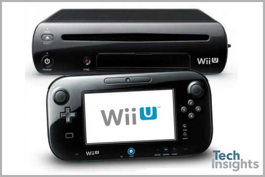
Nintendo Wii U
Looking at the Wii U Graphics Processor
Yes, even reverse engineering the latest technology has its up and down days.
At the start of the reverse engineering process, we generally have a simple electronics teardown before we can get to the more traditional tasks of helping our clients understand the process technology or circuit design of a chip. The routine of getting the devices in our offices, cataloging them in a database, cross-referencing the information to other design wins for market tracking, filling out lab work orders for depot, and analyzing the devices to find the latest process and circuit innovation is enough to make the teardowns we do seem like…well…work.
But every once in a while something really interesting happens. This is one of those times.
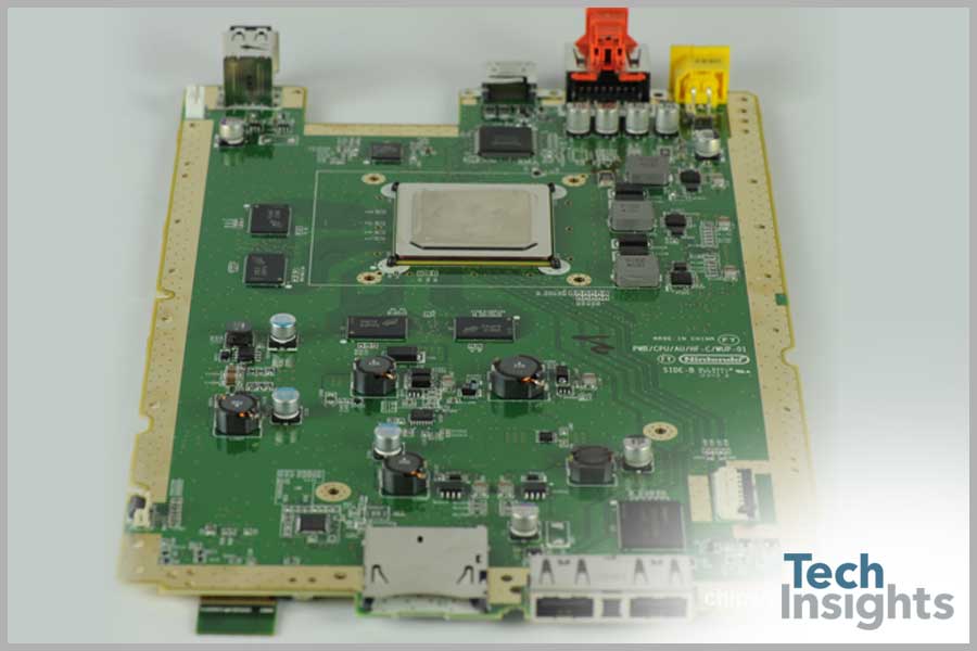
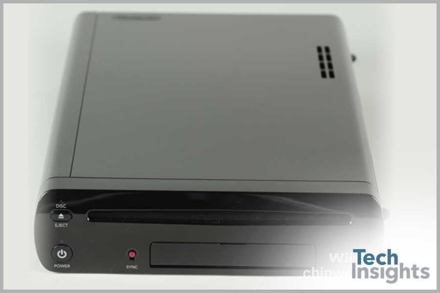
Nintendo Wii U Board
Late last week we discovered a gaming message board called Neogaf where they were crowd-sourcing funds to buy die photos of the multi-chip CPU/GPU package in the Nintendo Wii U. They had raised enough to purchase top metal die photos of the CPU, the GPU and the tiny NOR memory chip.
To a manufacturer of said chips, these types of top metal die images are useful, but for the purposes of analyzing the specifications, you need to go a little lower and look at the polysilicon layer. Rather than have the community continue to raise money, we thought we would step-in and help out. Since (at the time of publication for this blog) we are only 1 day away from the release of Dead Space 3, we thought that the gaming community might be able to put their funds to better use.
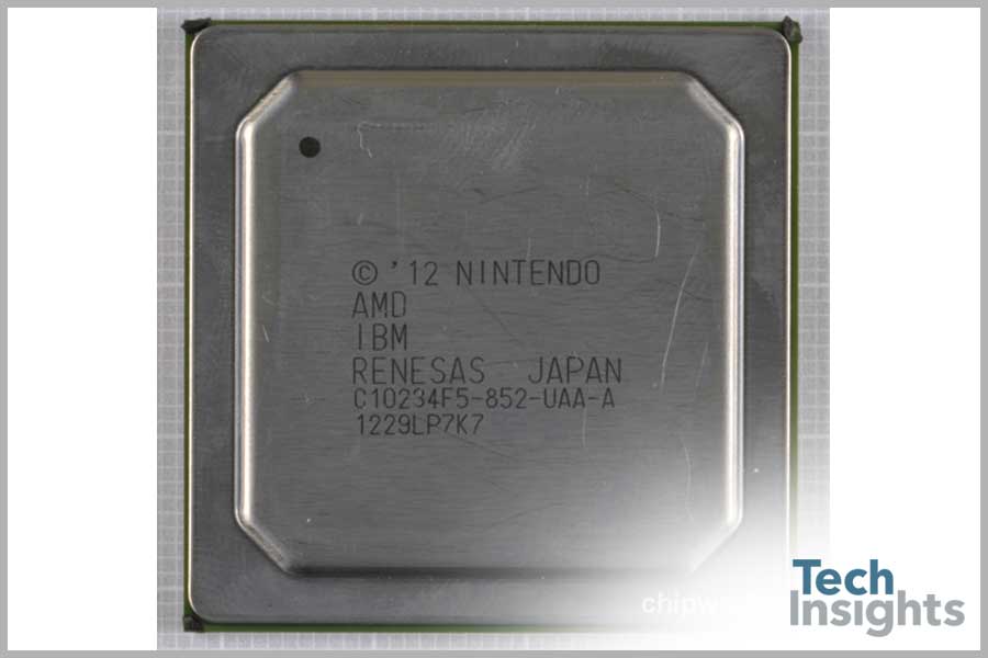
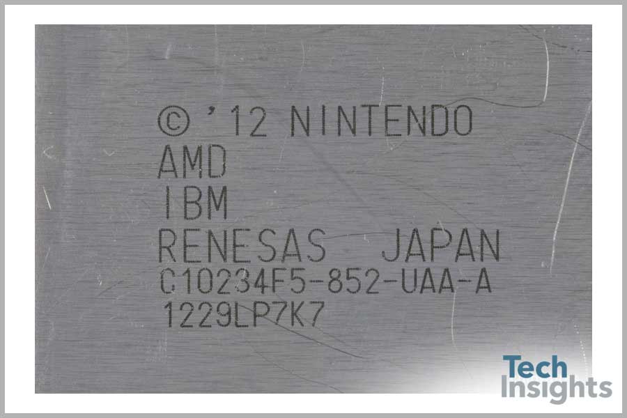
Nintendo Wii U C10234F5
About the Nintendo Wii U C10234F5 and why they were interested
It seems that Nintendo has not been disclosing very much information about the raw specifications of their latest console. This makes sense because they probably don’t benefit much from trying to compete on specifications against the latest “Asus ROG ARES II dual 7970 liquid cooled GPU in CrossfireX mode“ – and don’t worry, if you don’t know what that is then it probably means that you get outside regularly and have a relatively low home power bill.
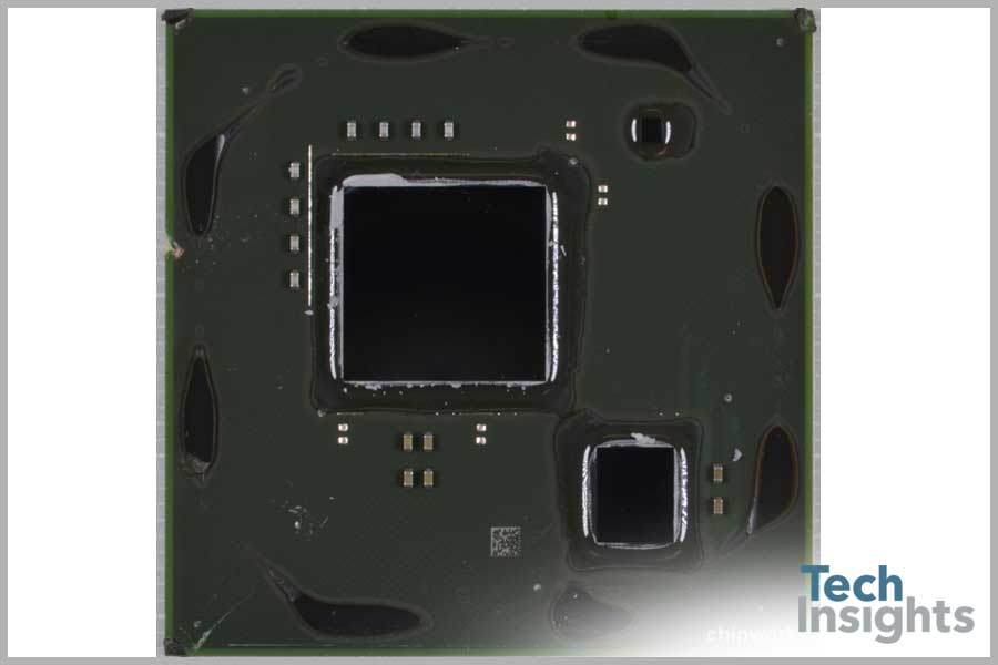
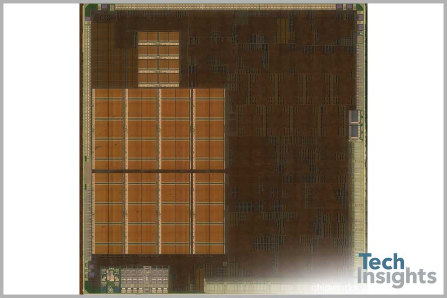
WiiU Graphics Processor - Polysilicon Die Photo
Nintendo prefers to focus on the holistic fun and the playable experience of their console and games, rather than delivering the most pure first-person shooter experience. That’s likely why they don’t publish techie details like graphics specs. Well, techie people love techie things and the act of keeping mute on details only fuels debate and discussion.
So without further ado, here is a look at the polysilicon die photo of the GPU from the Nintendo Wii U. We aren’t going to annotate the blocks because several people on that board (and probably elsewhere) have already been volunteering to take on the task. After all, we are giving away the die image, so we should let them do their own reverse engineering annotation. The image below is only a thumbnail and you can click on it to get one that is higher resolution.
The die size is ~12.0 x 12.5 mm. (~150 sq. mm.), compared with ~117 sq. mm. for the earlier Wii Black. You can feel free to re-use it on your site but please ensure the watermark remains intact. If you are highlighting a single area of the die, please provide proper accreditation.
Nintendo Wii U Quick Cost Estimate
Wii U Game Pad
| Display | $24.75 |
| Main GamePad Components | $30.00 |
| Other Parts (Battery, WiFi casing, etc) | $24.50 |
| Total | $79.25 |
Wii U 8 GB Console
| Processor | $40.00 |
| Optical Drive | $17.00 |
| Flash Storage | $6.00 |
| RAM | $6.00 |
| Other Parts (WiFi Chips, Bluetooth, Casings, etc.) | $79.38 |
| Total | $148.38 |


