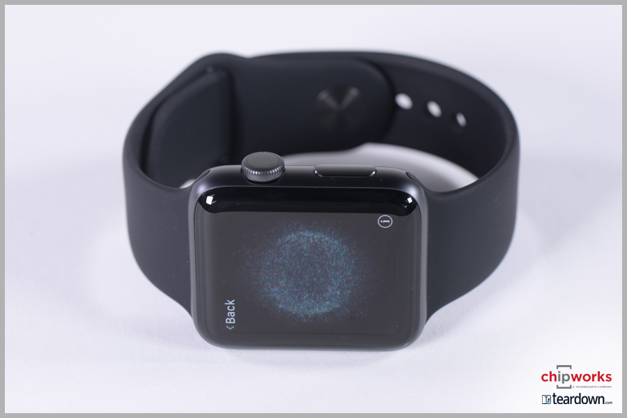
Apple Watch Series 2 Teardown
Posted: September 28, 2016 - Updated: March 23, 2017
Contributing Authors: Mandi Gingerich and Jim Morrison
Just when you thought we might be finished with Apple-related teardown updates, here we are once again. We too had hoped to be through with this by now, but alas, there seems to have been a delay in delivery of our new Apple Watch. We’ve heard this is a fairly common experience this time around. Let’s see if it was worth the wait…
Apple Watch Series 2
What’s new?
The latest iteration of the Apple Watch, dubbed Series 2, has been upgraded to improve its functionality as a primarily fitness-tracker device. Only a hair thicker and weighing in heavier than the original, this Watch looks largely the same, until you turn it on and observe the brighter display.
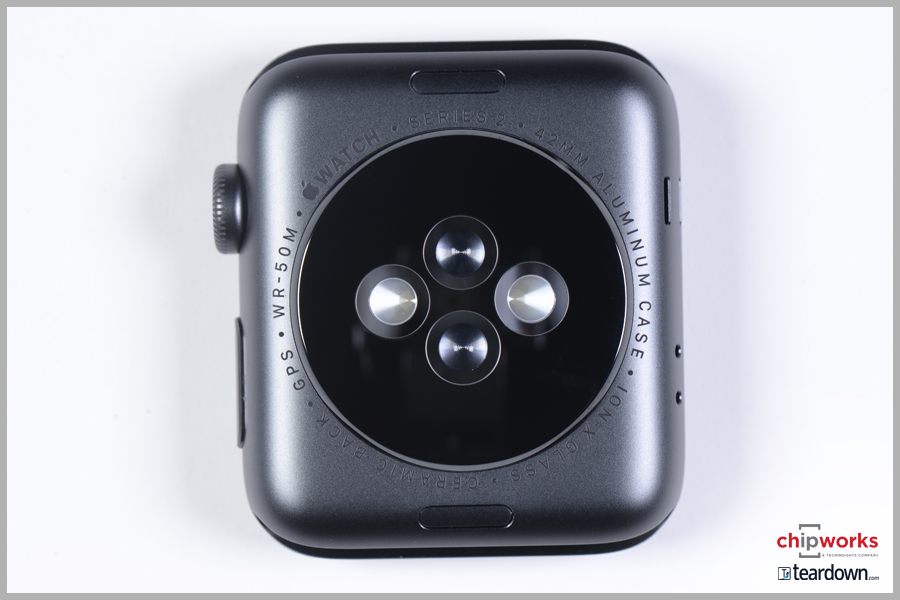
On the inside, the most notable changes include water resistance (up to 50 m), GPS, a faster processor, longer battery life, and the new watchOS 3. The previous generation, now known as Series 1, has likewise received an upgraded processor and OS.
Inside the Apple Watch Series 2
What's inside?
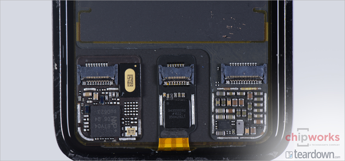
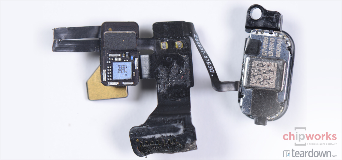
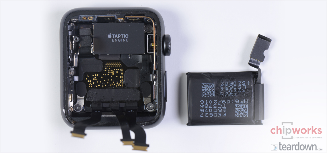
It doesn’t take long for this Watch to reveal some of its secrets. Others will prove more trying, but more on that later. Below the display (in our case, the 42 mm version), we can already see a few pieces including an Analog Devices 343S00092 touch controller, a Texas Instruments 36372 DC-DC converter, and an NXP 67V04 NFC solution, which contains the PN549 NFC controller and the “008” secure solution. In the original Apple Watch, the NFC and touch controller were found inside the S1 system-in-package (SiP). On the underside of the display, we see an optical sensor or an ambient light sensor from AMS. Behind the Digital Crown, we see that again STMicroelectronics has the optical encoder, a motion sensor for optical finger navigation (OFN).
STMicroelectronics
Behind the Digital Crown we see again that STMicroelectronics has the optical encoder, a motion sensor for optical finger navigation (OFN)
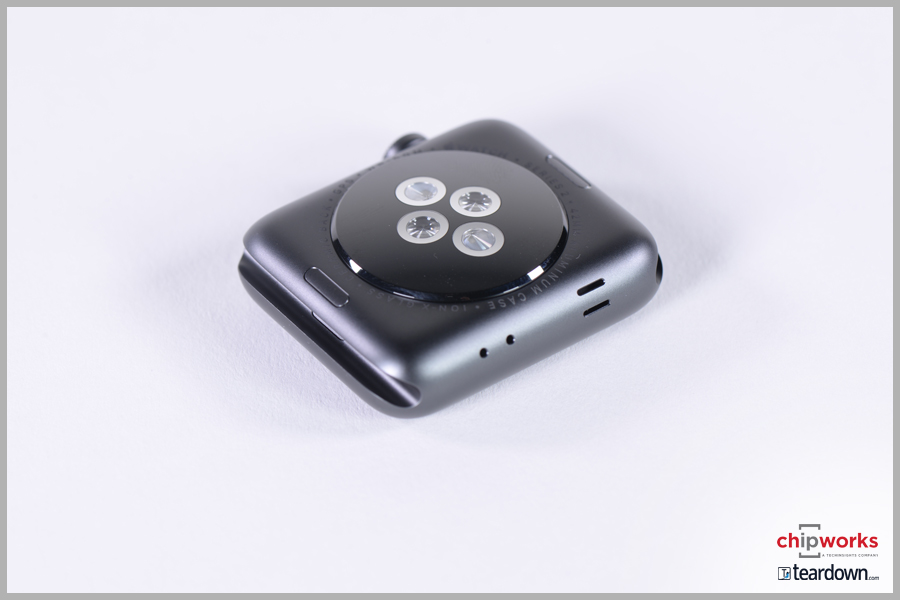
The Force Touch module
The Force Touch module
Digging a little deeper, we find the Force Touch module. We’ve written about this technology at length in the past, including a new exploratory functional analysis of its implementation in the iPhone 6s, and we don’t see anything new in this Watch. Even the controller is the same Analog Devices AD7149 capacitance sensor controller we have observed in previous generations of Apple Force Touch-enabled devices. Again, in the original Watch, this was found inside the S1 SiP.
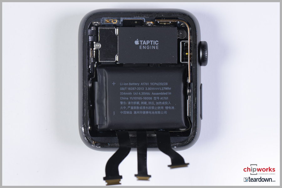
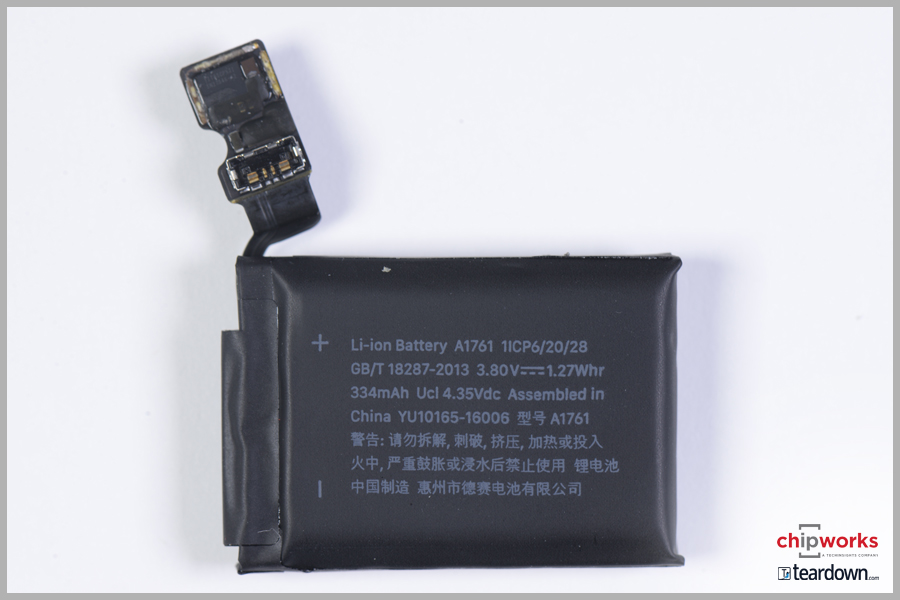
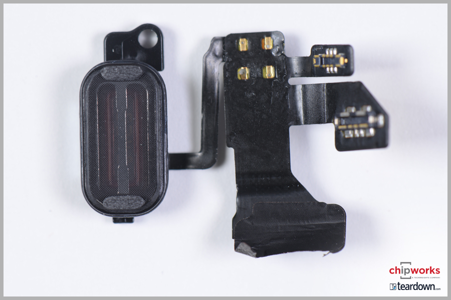
Taptic engine and battery
Taptic engine and battery
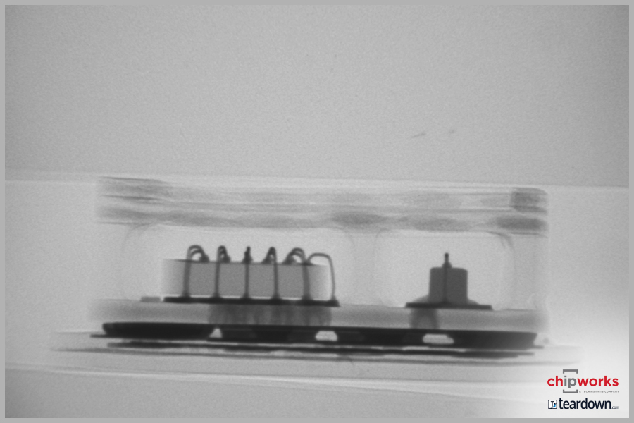
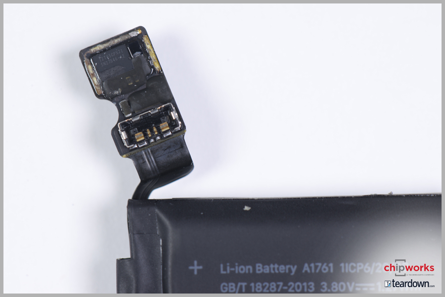
Next up is the taptic engine and battery. As our friends at iFixit note, this battery is not easily removed due to a large quantity of adhesive, though this will prove to be only the first in a series of challenges presented by this teardown. Once we get it out, we see that the longer battery life of the Series 2, despite power-sucking GPS and a brighter display, can indeed be attributed to a larger battery. The 42 mm model clocks in at 3.80 V and 334 mAh, for 1.27 Whr of power. Attached to the battery’s flex cable, we find a Texas Instruments SN27546-A2 single-cell Li-ion battery fuel gauge.
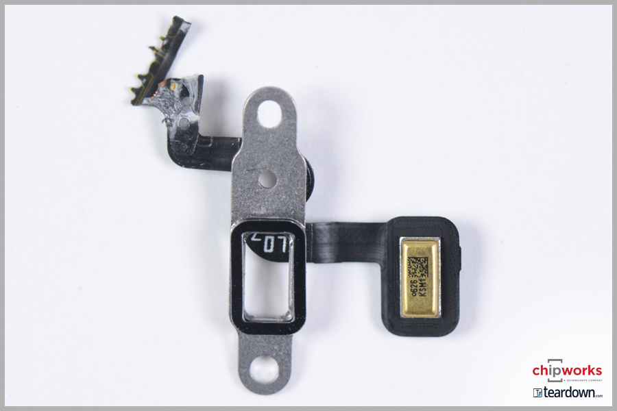
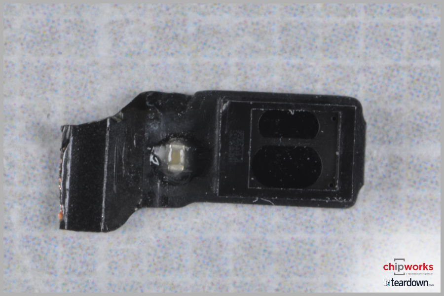
Microphone and speaker
Microphone and speaker
Along the way, we also found a Knowles KSM1 microphone and a nifty water-resistant speaker. When the Watch is unlocked from water use, the speaker, which is designed to flood with water, will vibrate to eject that water. Early reviews of the watch have noted that this is actually audible and very small droplet can be seen exiting the side of the Watch (the speaker opening is a dual-slit on the left side).
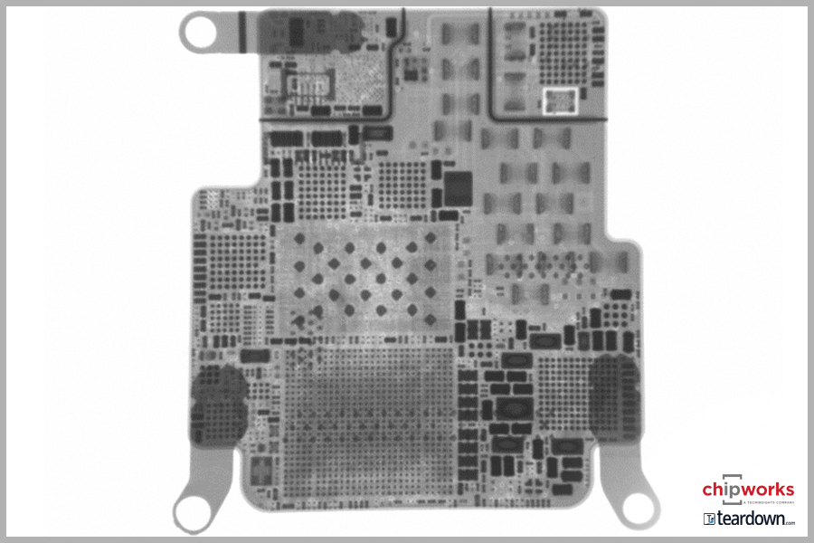
So what about the S2?
As you may have guessed by now, this is where we have once again run into some difficulty. If you’re a regular follower of our teardowns, you may recall the S1 SiP also proved a challenge to open up and identify the contents. Our labs are still busily working on it, and we’re confident they will come through, but here is what we can tell and show you in the meantime:
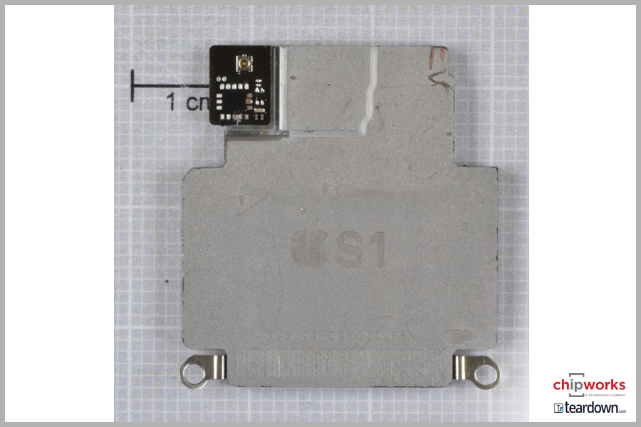
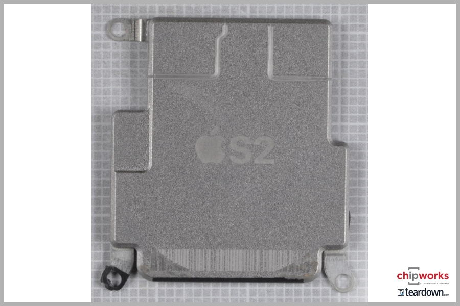
Comparing to the S1, the overall size remains about the same, though as we have already seen, a couple parts once found inside the SiP are now found externally: the capacitance sensor controller (Force Touch), NFC solution, and MEMS motion sensor.
Still MIA from our teardown of the Series 2 so far are the GPS/GLONASS, Wi-Fi, and Bluetooth solutions, as well as the processor. We expect we will find these inside the S2, of course, and will update you as soon as we are able to identify them. Please stay tuned.
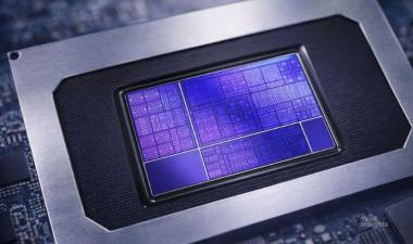
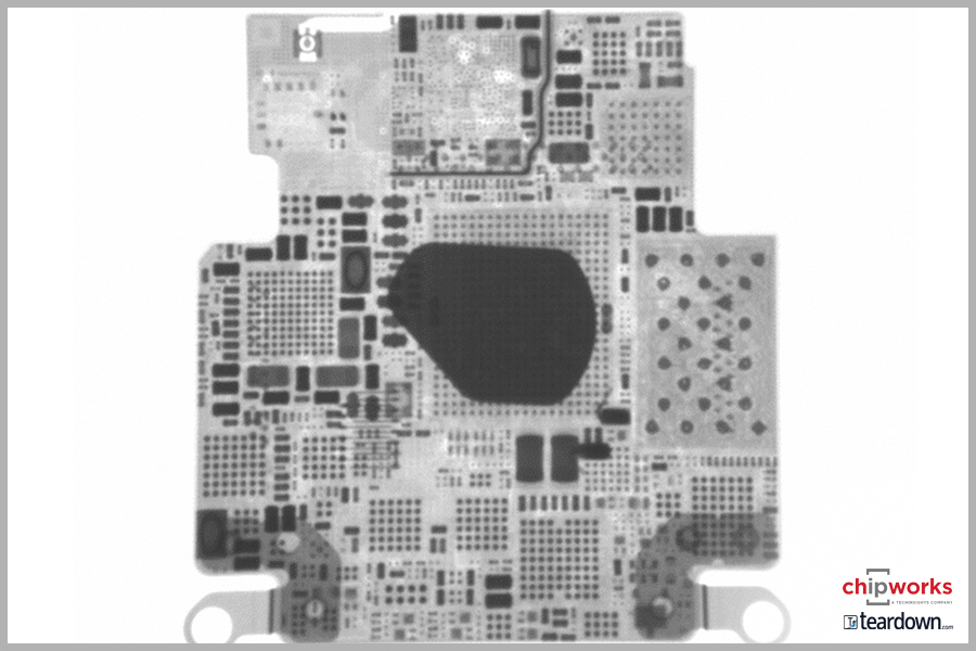
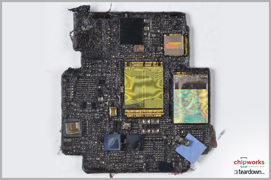
Update! The following is an image of the Apple S2 module after plasma etching to expose the internal die.
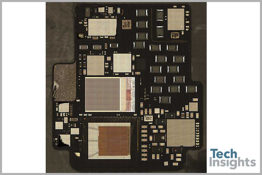
Image courtesy of JIACO Instruments
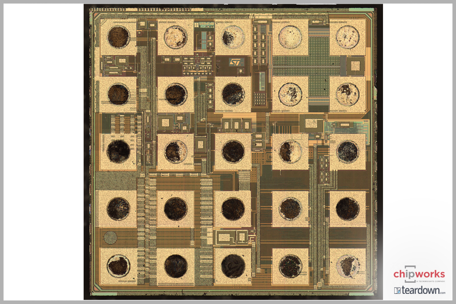
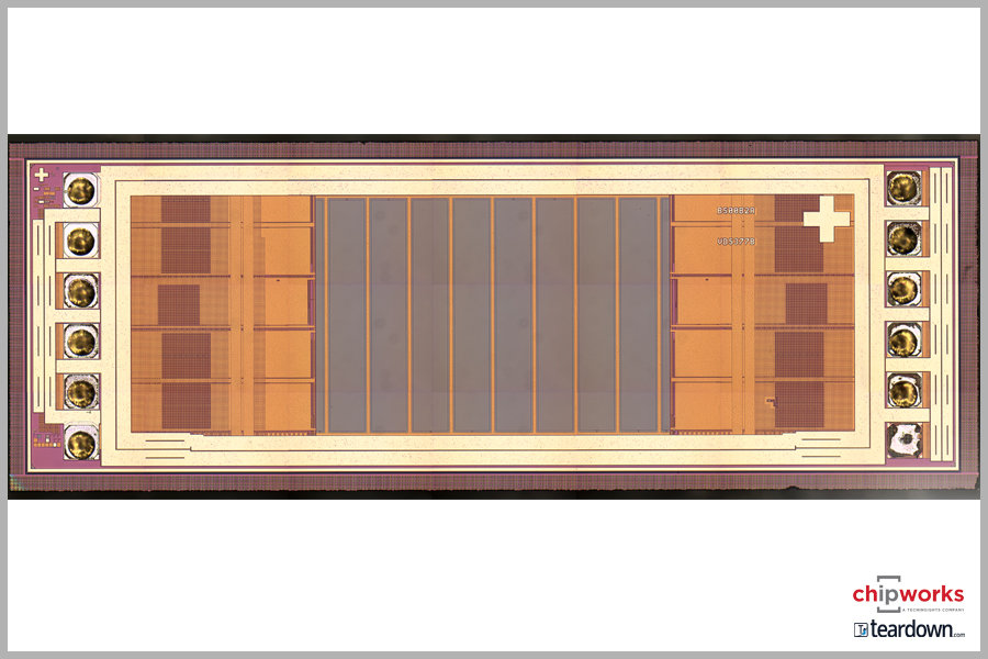
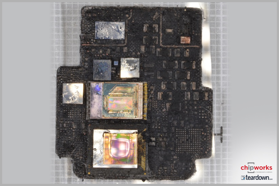
Update: The S2 contains more than 42 die!
The S2 is a system in package (SiP). As we learned with the first generation S1, these SiP modules contain a mix of package styles all in one large module. Similar to WiFi modules from Murata or USI, there is one module that contains several components. These components can be packaged as bare die (CSP, WLP etc) or traditional wire bonded packages to even multi-chip packages like a package on package or a multi die memory DRAM or NAND.
Deprocessing these SiP modules while still retaining package marks is a challenge. Care must be taken to capture every component in the SiP. The S2 contains more than 42 die! That is a lot of silicon in such a small module.
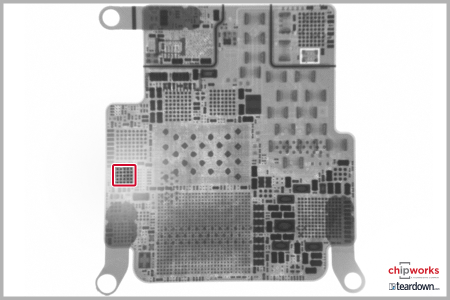
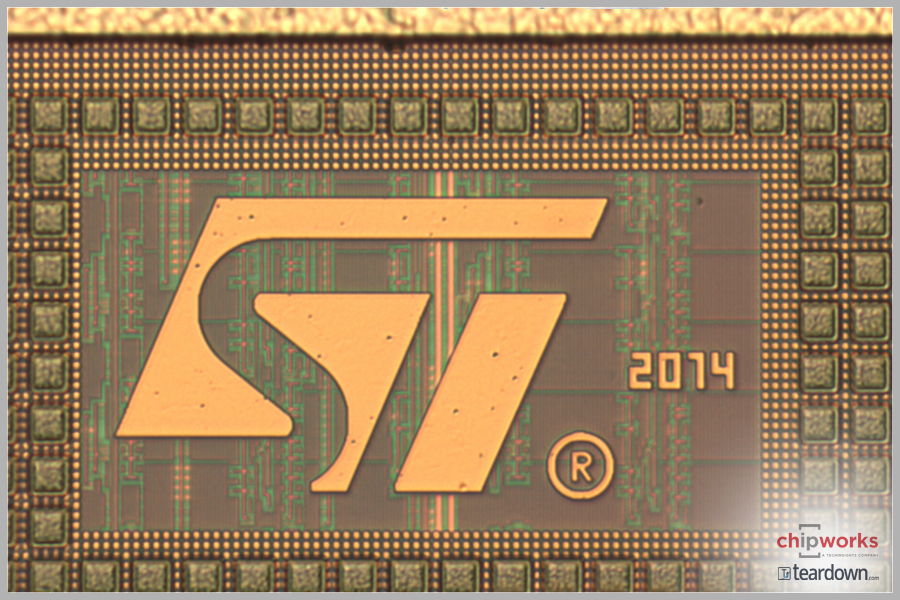
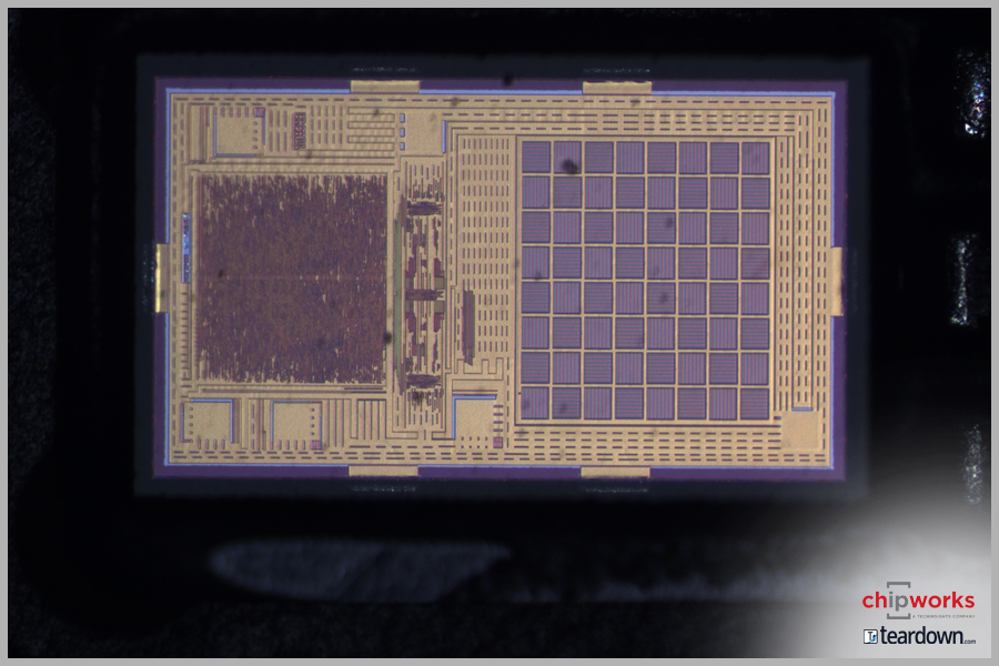
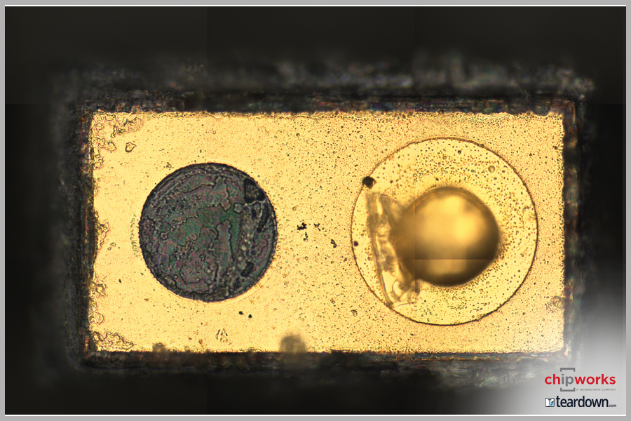
One of the first die to emerge from the S2 SiP is an STMicroelectronics ASIC. This die appears to be a custom ASIC for the Apple Watch series 2 to monitor various signal levels for the entire Watch. The die is 1.7 mm x 1.7 mm in a 5 x 5 CSP package.