Apple iPhone 7 Teardown
Posted: September 15, 2016
Contributing Authors: Stacy Wegner, Al Cowsky, Chad Davis, Dick James, Daniel Yang, Ray Fontaine and Jim Morrison
And the winner is….Intel, at least in the iPhone 7 A1778 we have in our lab. The Intel and Apple iPhone 7 rumors have been circulating around for a while, but from our experience, we know better not to believe everything we hear. However today seeing is believing and we have indeed found an entire Intel mobile cellular platform inside the iPhone 7. Intel supplied not just one, but two RF transceivers, the baseband modem, and the (RF) power management IC. Murata is another notable absentee in the RF front end, being replaced by Skyworks for the diversity receive modules. They do have the WiFi win, though.
The TDK-EPC filter banks may still help Qualcomm get in on the iPhone 7 action. In the past we have found Silanna Semiconductors, now Qualcomm, in the TDK-EPC modules. Our labs will help confirm this soon.
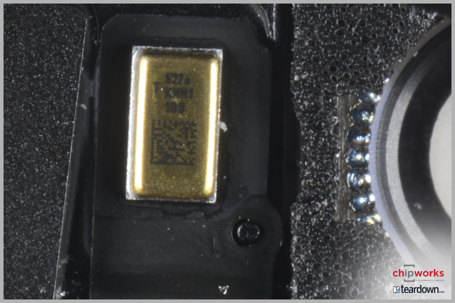
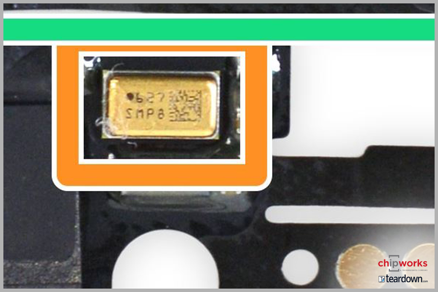
It’s not all about RF wins and losses. We confirmed the Apple A10 processor in our iPhone 7 is a TSMC chip, and we are currently looking to identify the die node technology, so stay tuned. We also found a win for MegaChips, (formerly SiTime), with one of their MEMS clock ICs. We have found MEMS clocks in mostly Wearables and some game controllers, but not many in our mobile device teardowns.
Find content like this and more in the TechInsights Platform. Sign-up for free today.
>
Costing
The iPhone 7 sees a number of cost impacting advancements over the iPhone 6S. The baseband parts (A10 and Intel PMB9943 LTE Modem) are more powerful,and more costly to make than their predecessors in the iPhone 6S. The storage memory has grown from the 16GB in the iPhone 6S to 128GB in the iPhone 7, representing another cost increase. The display/touchscreen actually decreased in cost, due to the fact that display costs have dropped since the iPhone 6S cost estimate was made a year ago. The cost estimates on the iPhone 6S are approximately 9 months old and are a snapshot of costs at that time; they will tend to drop over time as well. It is important to note that these preliminary market cost estimates, are by nature, based off of a less rigorous analysis than the costs derived from a deeper analysis.
Inside the Apple iPhone 7
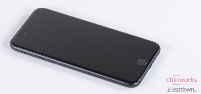
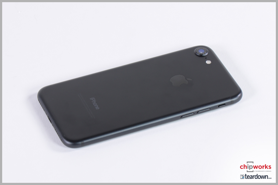
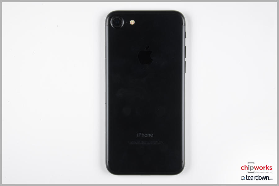
External
Apple iPhones have garnered a fair share of admirers, especially from their closest competitors like Samsung, Huawei, and even Xiaomi. But if it looks like an iPhone, feels like an iPhone, acts like an iphone, and is missing a headphone jack - then, it is an iPhone 7 (or iPhone 7 Plus).
The omission of the headphone connector may have freed up some precious internal design space, but whatever BoM and test savings were garnered were at least partially spent with the lightning headphone adapter Apple is supplying with every iPhone 7 and iPhone 7 Plus.
Just a few more words on the external features before we move on to the inside design. Apple made it a point to highlight the ‘new antenna’ design being part of the enclosure. What we think Apple meant was you just can’t see the antenna from the outside. For quite sometime now the RF antennas have been designed as part of a phone’s enclosure, and that is not just unique to Apple phones. It is just as likely to find an antenna designed within a phone’s enclosure as it is to find a phone with a separate antenna element. Like always we will be taking a close look at the X-rays and the enclosure to see if there is something more to this story.
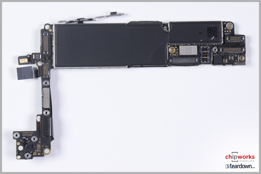
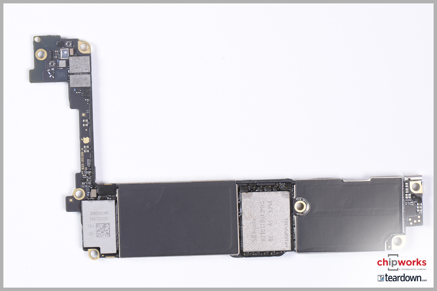
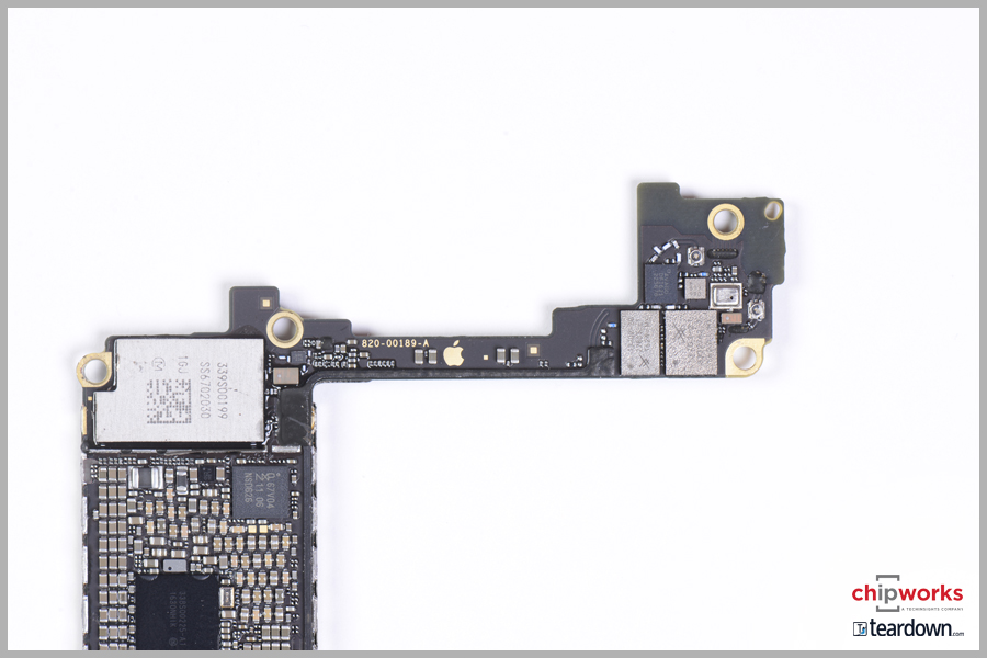
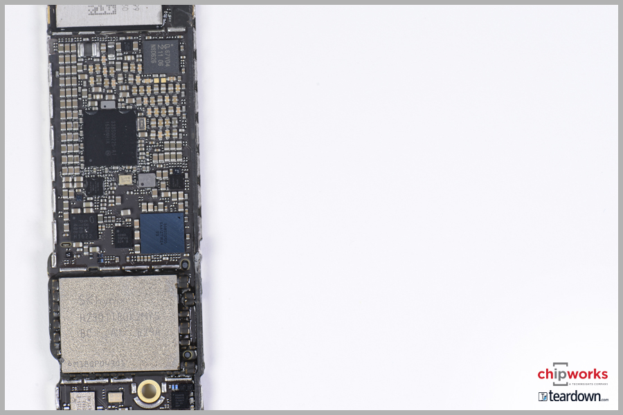
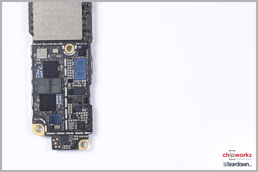
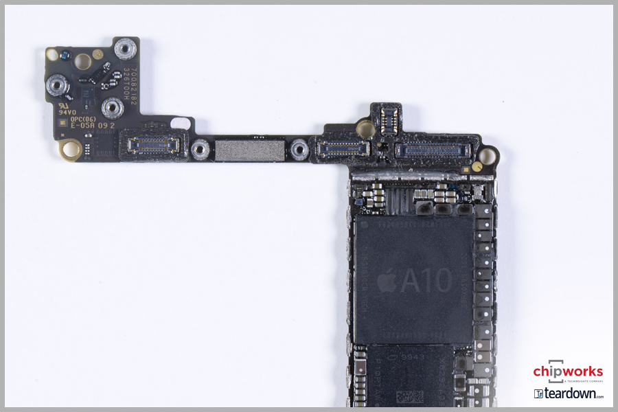
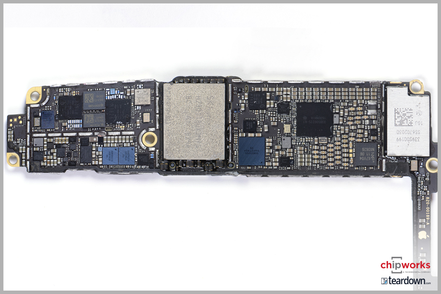
Board shots
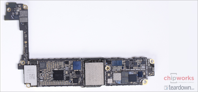
Apple iPhone 7 Board Shot
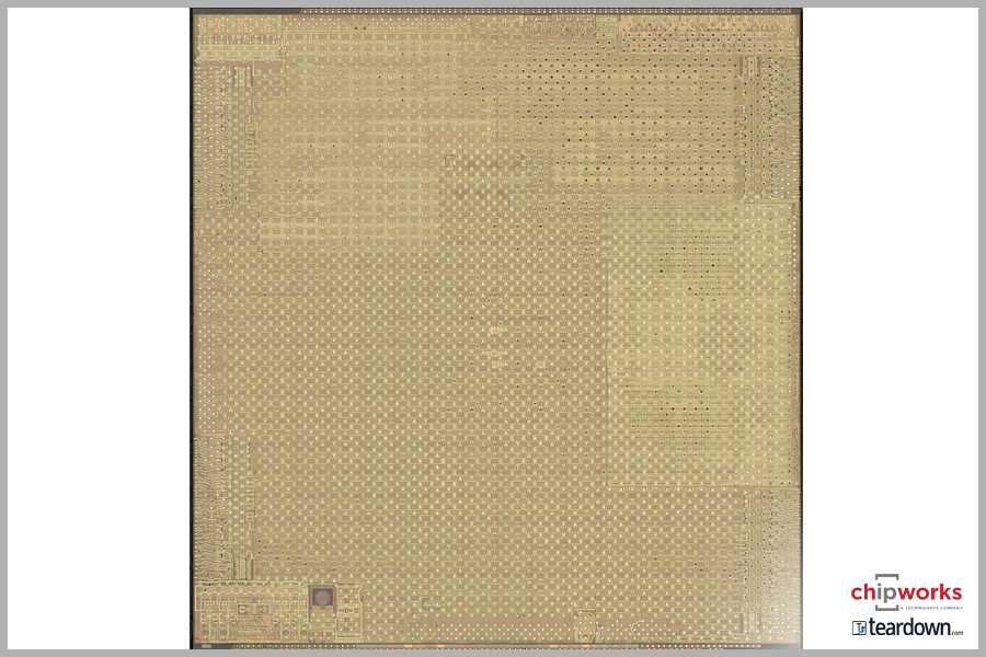
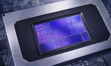
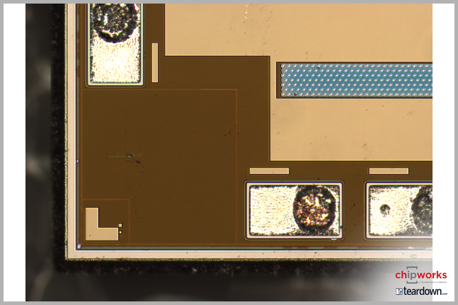
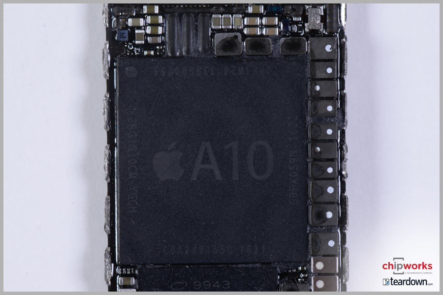
A10 Fusion Processor
A10 Fusion Processor
Apple’s part number for the A10 is APL1W24, 339S00255 vs the Apple A9, which was APL1022, 339S00129. We are not certain what the addition of the ‘W’ in the new number signifies. As we mentioned above, our iPhone 7 A1778 had an A10 application processor from TSMC. If you remember on the iPhone 6S, both Samsung and TSMC supplied the A9 processors. As of this writing we do not know if that is still the case, or if the A10 is being single sourced from TSMC.
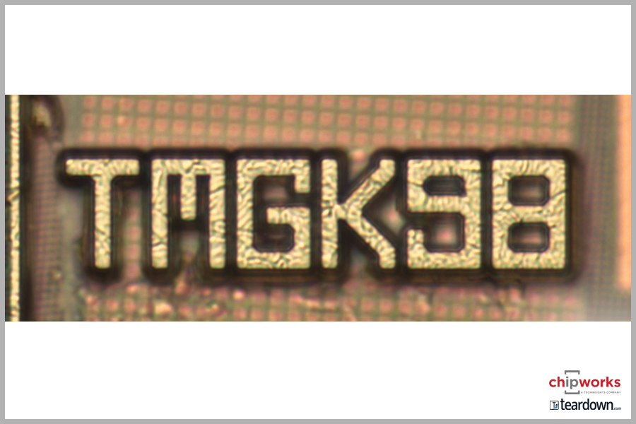
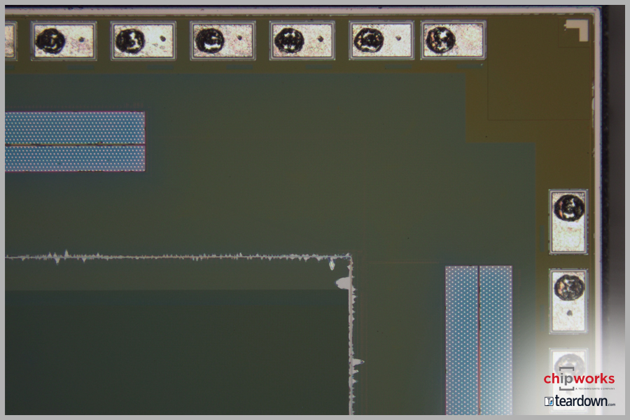
Our die photo of the A10 shows a die part number of TMGK98 which is continuing up in sequence from the A9’s TMGK96. The A10 die size is ~125 sq. mm with a reported 3.3 billion transistors.
We have confirmed the process to be TSMC 16FF-based, so this means that Apple has basically been in the same 20/16nm technology for the last 3 generations, and it took 2 iterations on FinFET for Apple to get the A10 back to the gate densities we saw in the A8, optimized on a planar process.
A notable difference from the A9 to the A10 is much tighter SoC-level die utilization, which is more in line with the A8. This, along with tighter 9-Track and 7.5-Track libraries of an 16FFC process, are expected to have kept the die from bloating to the ~150 sq. mm level that we were expecting from a straight scale of the A9 to the A10, in terms of transistor count.
It has been impressive how architectural and design techniques have exploited the device-level performance boost from 20nm planar to 16FF FinFET, and the expected improvement in 16FFC, to continue the speed improvement and power reduction, despite the lack of gate-level scaling. This goes to show that there is a lot more to SoC optimization than just scaling, and makes it all the more important to understand how to best squeeze performance out of the latest or previous technology nodes.

A10 Fusion Processor
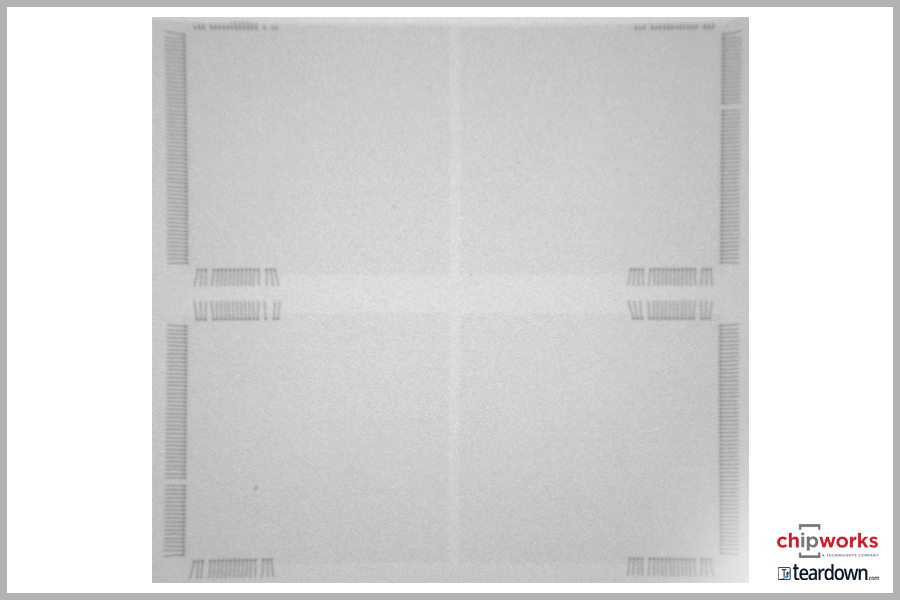
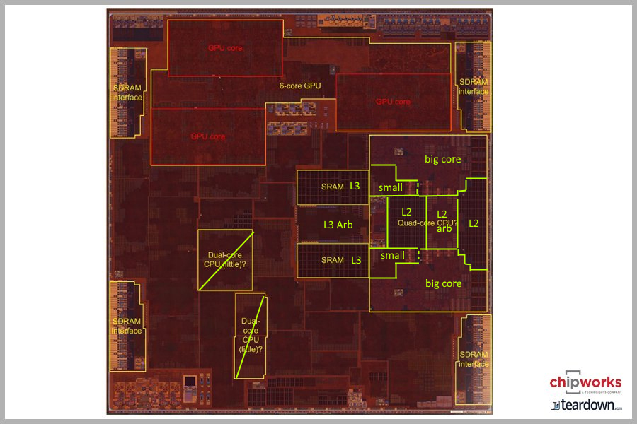
Now we have a transistor-level die image, and we can see the circuit blocks, so here is our conjecture as to what we have:
We’re pretty sure about the GPU and SDRAM interface blocks, but for us the question is, where are the two new low-power cores announced by Phil Schiller during the launch last week?
We are looking for two pairs of cores that are usually symmetrical in layout, and the large high-power cores are fairly obvious on the right side of the die image. However, they take up ` ~16 mm2, compared with the ~13 mm2 used by the A9 cores; so do we have more powerful and larger high-power cores, or are the “little” cores integrated with the “big” ones in the same area, on the left of that block? The existence of two large blocks of SRAM in there (compared with the A9’s single area) provides some support to that theory.
On the other hand, we have two other twin blocks that we have marked up that could also be CPU cores. We need further investigation, or reader information gratefully received!
A10 Fusion Processor
UPDATE: We have revised our first A10 floorplan with help from our friends at AnandTech in the search for the small, high-efficiency cores. Our combined guess is that it is likely they are indeed integrated within the CPU cluster next to the big, high-performance cores. This makes sense given the the distinct colour of the small cores indicating a different digital library, and the position of the big core L1. Thanks to our friends over at Anandtech for reviewing the floor plan with us and providing input on where these blocks might be located!
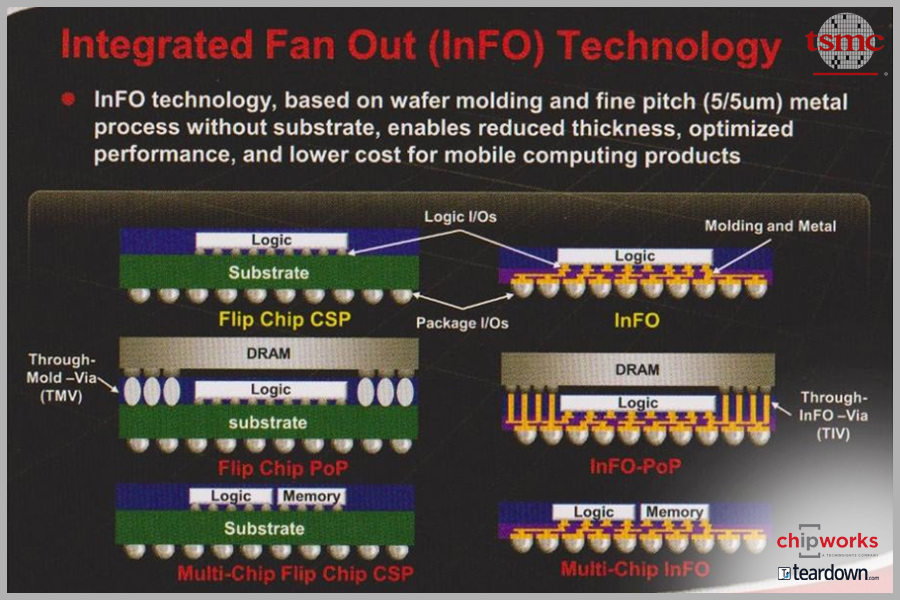
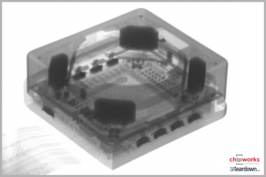
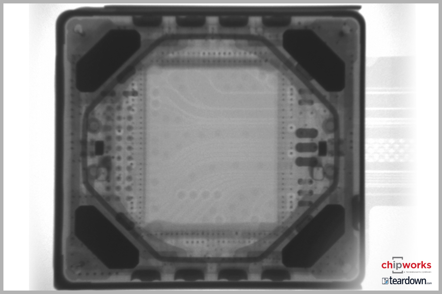
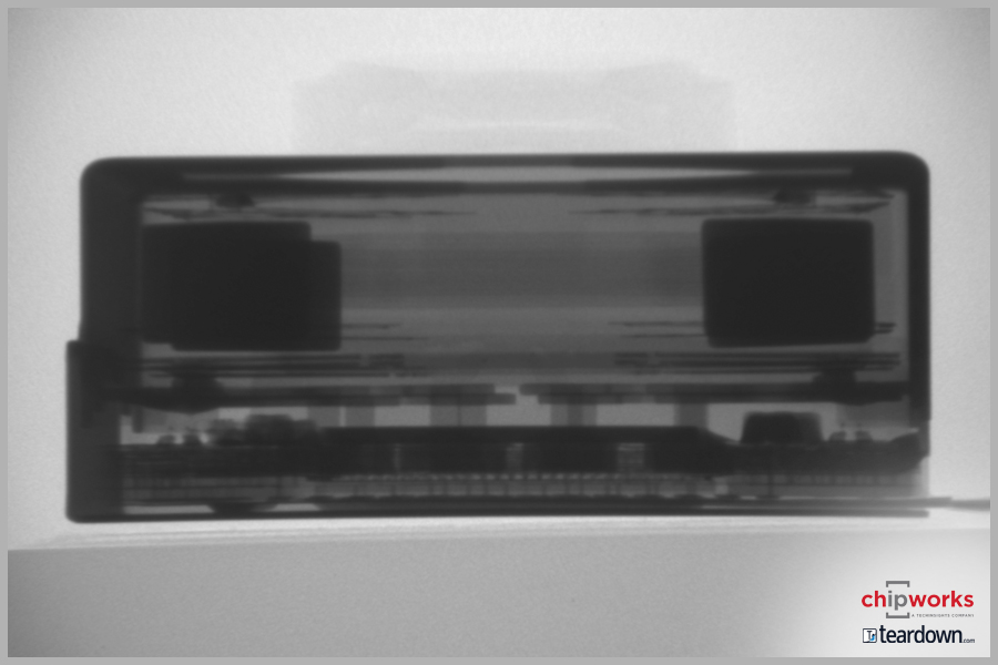
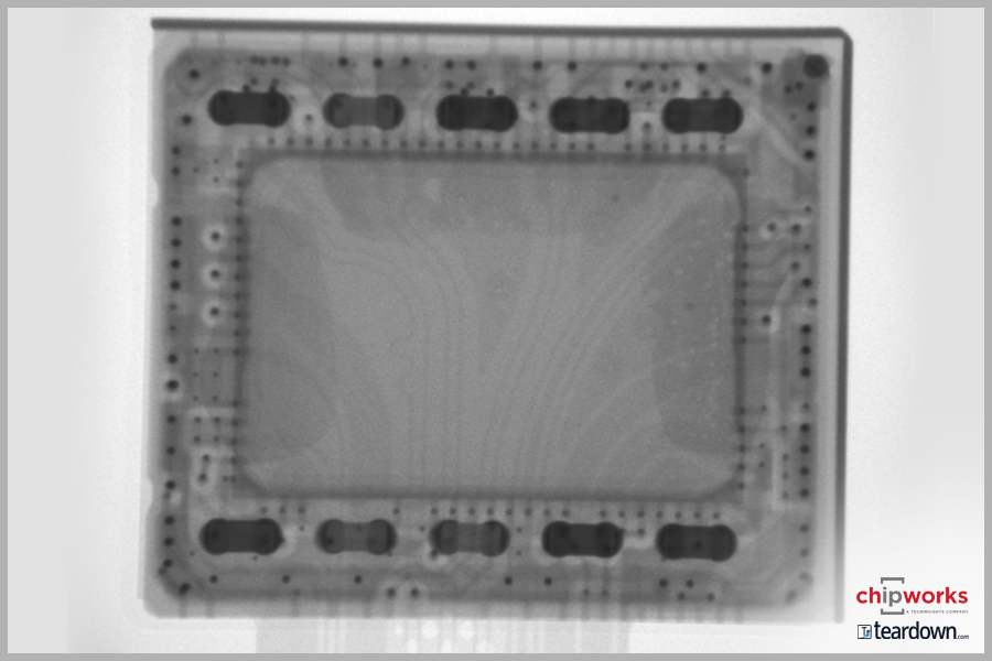
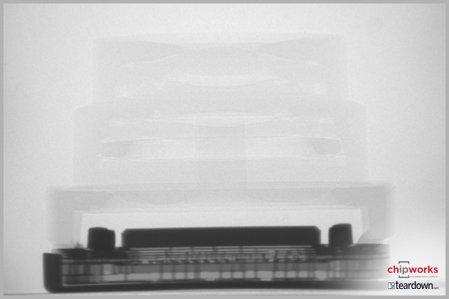
Beyond the die, one important factor for performance, has been achieved via packaging. The A10 processor is incredibly thin, giving credibility to the reports that TSMC’s InFO packaging technique is being used.
The A10 sits below the Samsung K3RG1G10CM 2-GB LPDDR4 memory. This is similar to the low power mobile DRAM as the one we found in the iPhone 6s. Looking at the X-rays we see the four dies are not stacked, but are spread out across the package. This arrangement keeps the overall package height to a minimum. Assembled in a package-on-package assembly with the A10 InFO packaging technique reduces the total height of PoP significantly.
Baseband
Baseband
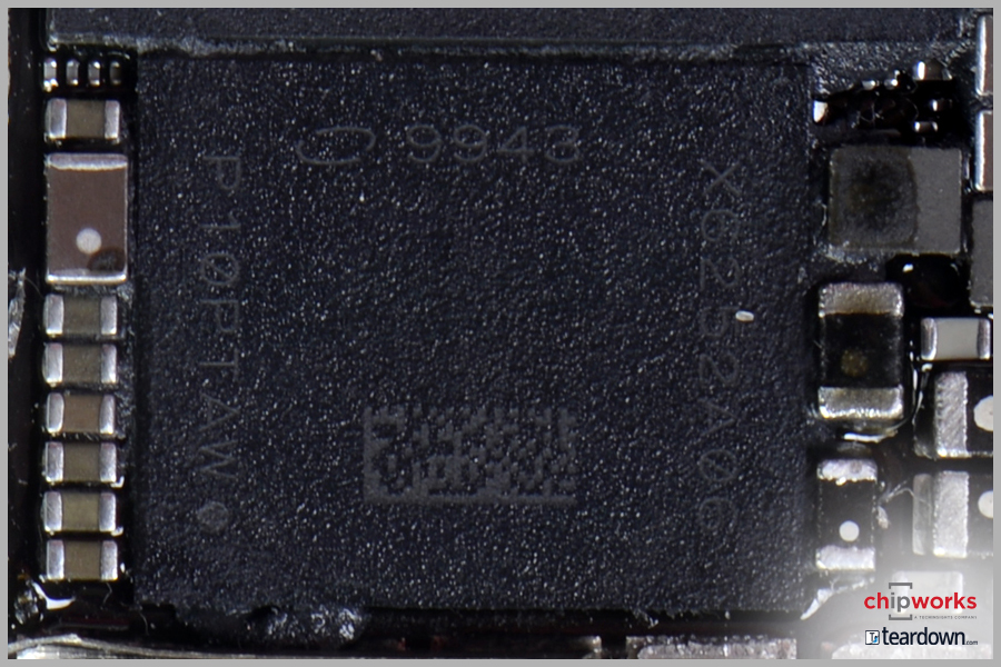
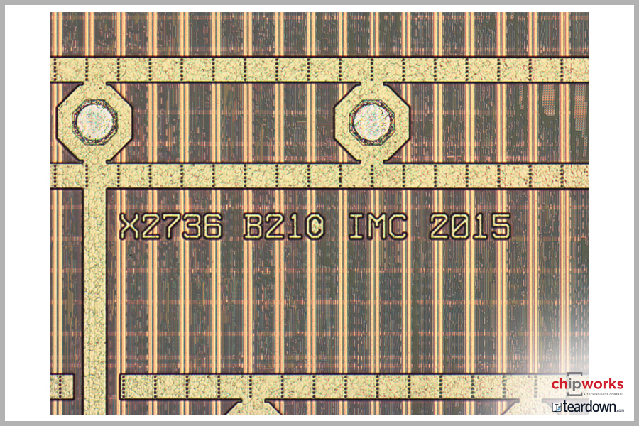
In the iPhone 7 Model A1778 we have torn down, we see Intel’s Baseband Processor (Modem) PMB9943. We suspect that this is the rumored Intel XMM7360 modem. We will decap it and shoot the die photo and update this blog as images become available.
UPDATE: our lab did an excellent work in depotting the Intel modem quickly. We have confirmed that it is Intel XMM7360. The modem die size is ~66.4 sq. mm.
What will be interesting at least to us, is whether we will find an Intel platform in the CDMA versions of the iPhone 7 and iPhone 7 Plus, or if Qualcomm will get the win. We will be doing a Deep Dive report on an iPhone 7 CDMA A1660 version to find the answer.
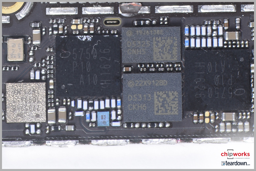
RF Transceiver
RF Transceiver
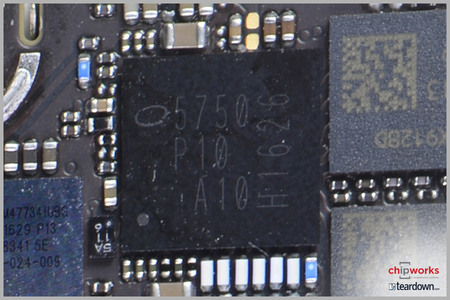
Intel continues their win in the iPhone 7 with two Intel PMB5750s, or what they call their SMARTi 5 RF Transceivers. Here again, TSMC wins as well, as the SMARTTi 5 RF transceivers are built on TSMC’S 28nm process (source: Linley Group Mobile Chip Report). TechInsights has done a circuit analysis report on a previous generation; the Intel PMB5747.
Power Management ICs
Power Management ICs
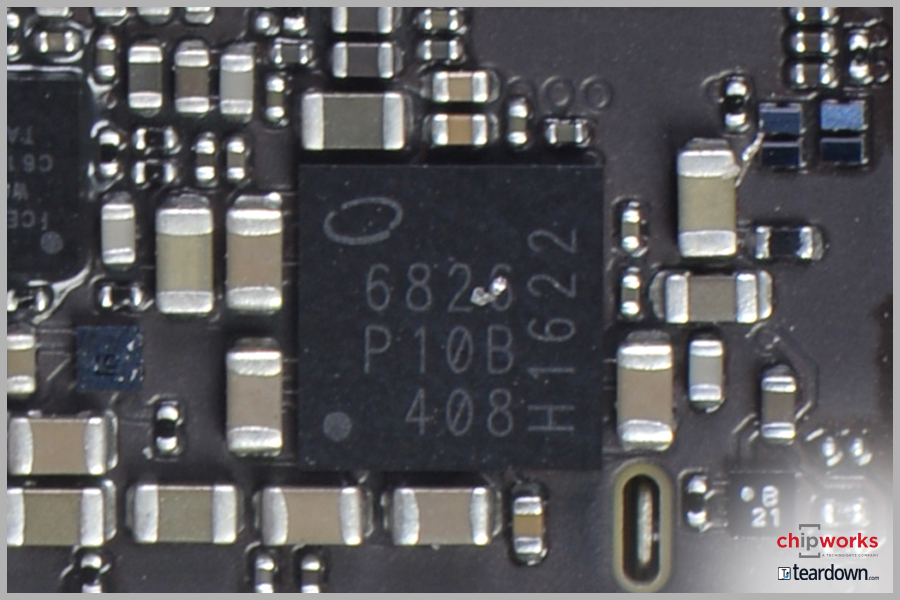
A newcomer, Intel’s PMB6826, otherwise called X-PMU 736 is found in the iPhone 7. Like the SMARTi 5 RF transceivers, the X-PMU 736 is part of Intel’s XMM 7360 platform.
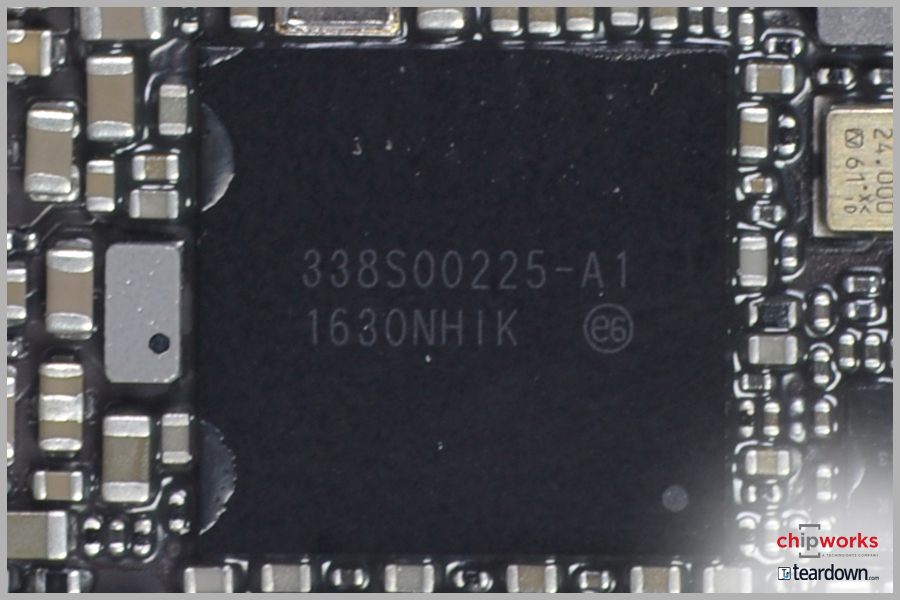
While Intel handles its own cellular ICs, Dialog continues to have a presence in Apple phones. Here we have the 338S00225, a new Apple/Dialog Semiconductor PMIC for the iPhone 7. For your reference, the previous iPhone 6S and 6S Plus used 338S00120 and 338S00122 respectively.
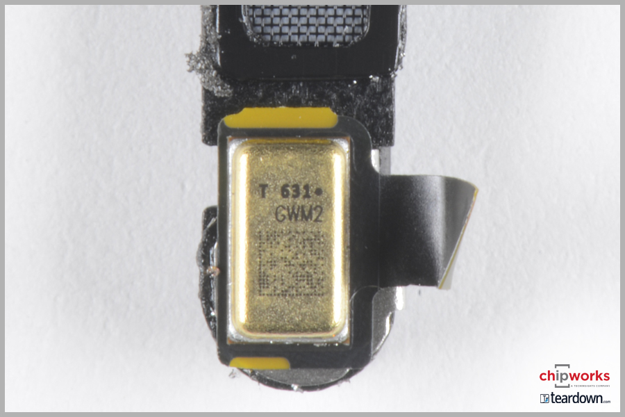
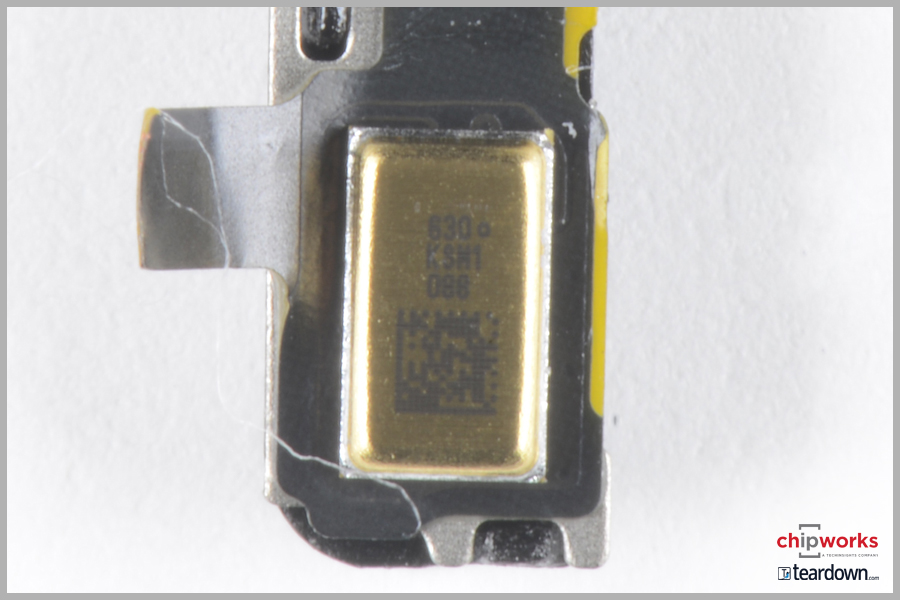
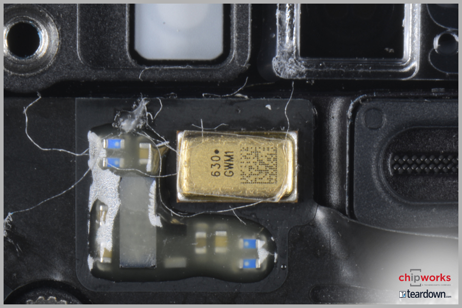
Microphones
Microphones
As per normal multi-source philosophy of Apple, the microphones are being supplied by a few well known qualified vendors. In our model A1778, we have two microphones at the bottom of the phone and two up at the top.
The microphones at the bottom are sourced by Goertek and Knowles. The microphones on the upper part of the phone are Goertek and Knowles.
Looking over at the iFixit teardown of the iPhone 7 Plus we see STMicroelectronics has also scored design wins into the iPhone 7 Plus.
eCompass
Flash Memory
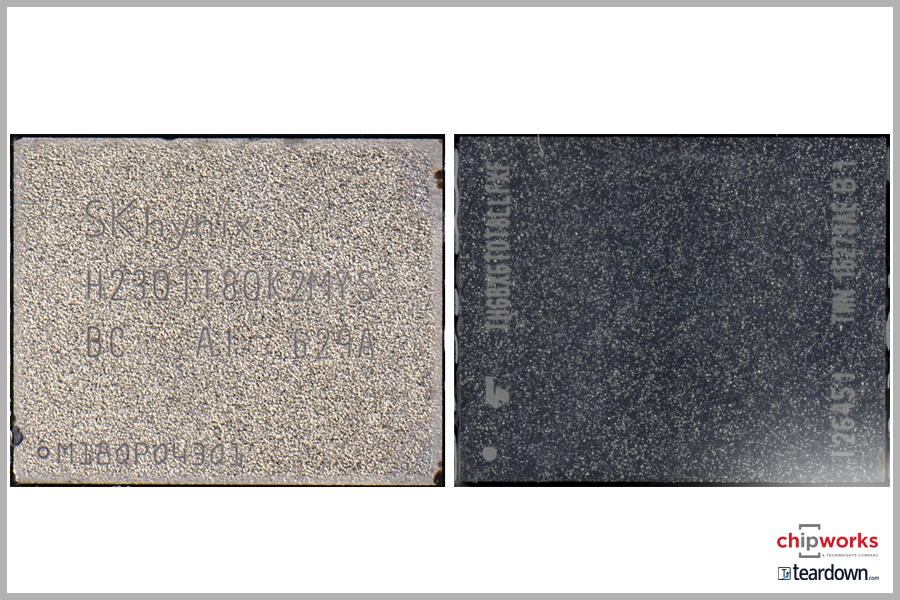
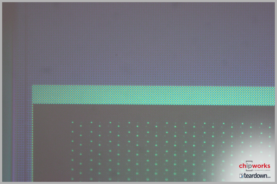
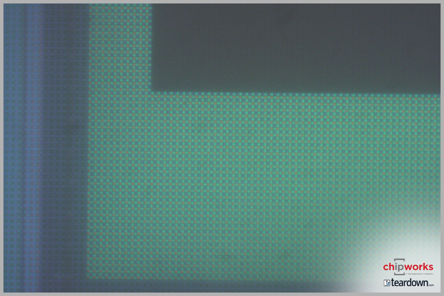
Since Chipworks and TechInsights have now joined forces, this is the first official quick turn of a 128 GB Apple phone for some of the participants from the TechInsights teardown team. This means for some of us, it is the first time we have seen an SK Hynix H23Q1T8QK2MYS 128-GB part with EMI shielding, fabricated in 15-nm technology. Our second phone confirms the memory is definitely being dual-sourced because it has a Toshiba THGBX6T0T8LLFXE 128 GB NAND memory IC also fabricated on 15 nm.
Rumour has it the 256 GB version of the iPhone 7 will have 3D NAND. This is what is expected since that will be a thinner eight-die stack of 256-Gb dies, as opposed to a 16-die stack of 128-Gb parts. The question is, will it be Samsung, Micron/Intel, or even Toshiba? Again, all answers we will uncover once we have completed our teardowns.
Update! The Toshiba 3D NAND was in fact found in the 256GB version of the smartphone we tore down.
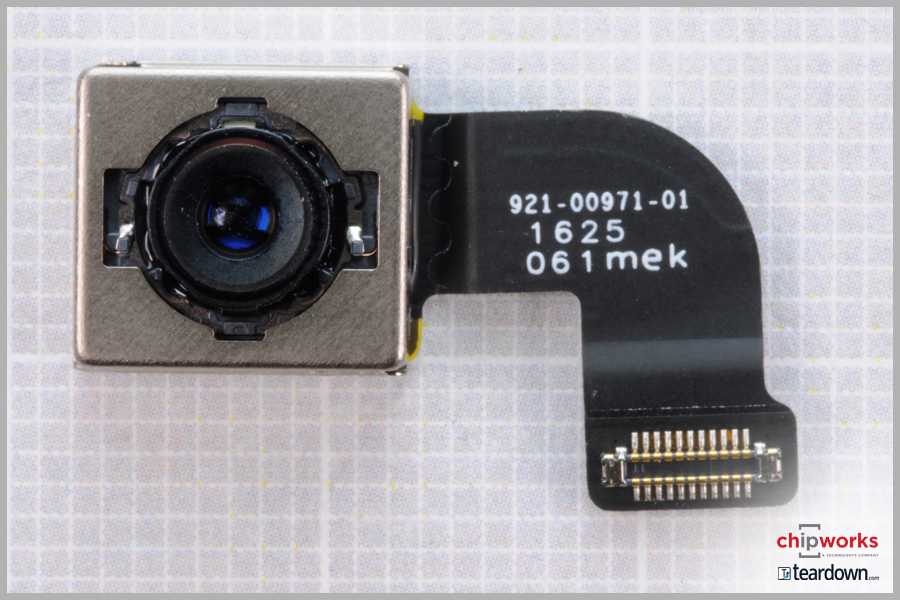
Camera
Camera
Cameras
Cameras have become such an important feature of any smartphone, and maybe even more so for the iPhones, Samsung Galaxy phones, now even Huawei is jumping all in with their dual camera on their latest flagship the Huawei P9. At this point, the camera of the iPhone 7 is in the lab to determine who made what, and the optical image stabilization source.
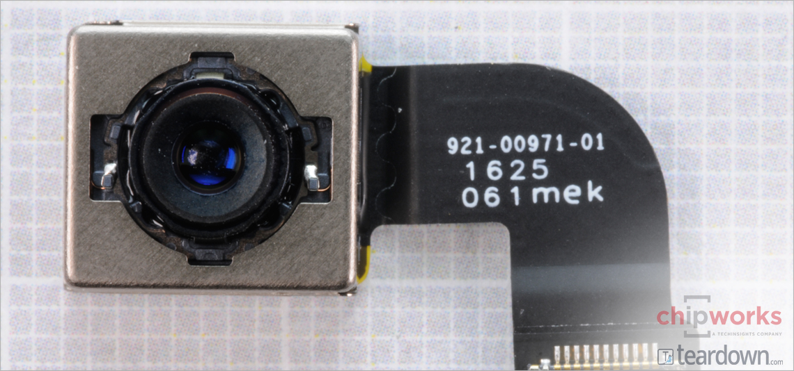
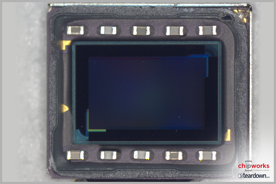
iSight Camera
iPhone 7’s iSight camera has a larger, ƒ/1.8 aperture, as compared to the ƒ/2.2 aperture used for iPhone 6s/6s Plus. The 10.6 mm x 9.8 mm x 5.7 mm thick iSight camera module features optical image stabilization (OIS) and a six-element lens. Although the 12 MP resolution and 1.22 µm pixel pitch hasn’t changed, the iSight’s camera chip is advertised as being 60% faster and 30% more efficient than its predecessor.
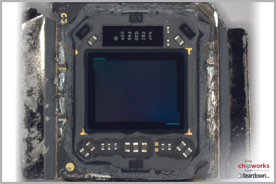
The iSight camera chip was sourced from Sony and fabricated using its Exmor RS technology platform. The 12 MP chip features a Bayer RGB color filter array (CFA) and embedded phase detection autofocus (PDAF) pixels. The die size is 5.16 mm x 6.25 mm (32.3 mm2) as measured from the edges of the die stack. We expect our planned analysis will show the CMOS image sensor (CIS) die to be fabricated by Sony in its 90 nm technology generation. The through silicon via (TSV) patterning tells us it’s a 2nd generation Exmor RS sensor and not 3rd generation Exmor RS with direct bond interconnect (DBI). The TSVs are used to connect the CIS chip to an underlying image signal processor (ISP), which is not to be confused with the complementary ISP functions embedded within the A10 chip.
We are anxious to see the results of our technical analysis of the iSight’s ISP. Sony originally stacked its Exmor RS CIS chips with 65 nm generation ISPs, then 40 nm and most recently 28 nm bulk CMOS. There have been rumors of Sony collaborating with GLOBALFOUNDRIES for stacked chip ISP production on 22 nm FDX, however with an announced mass production date of mid-2017 it is likely not in use in the iPhone 7.
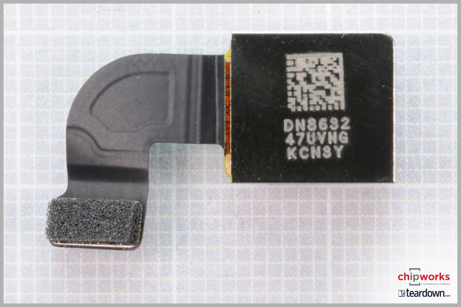
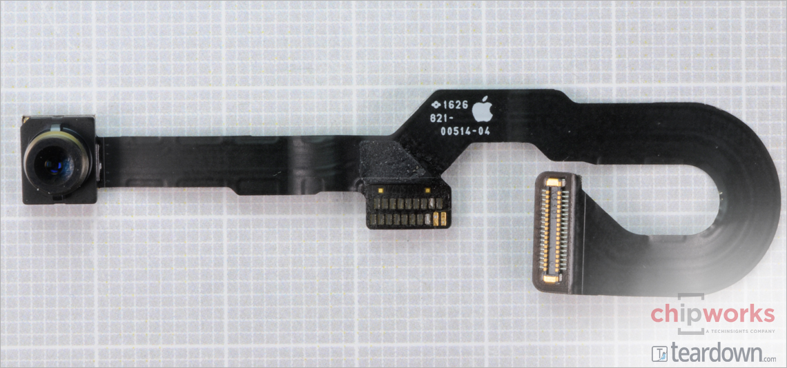
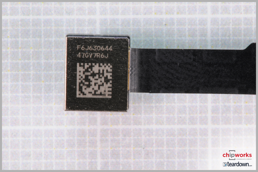
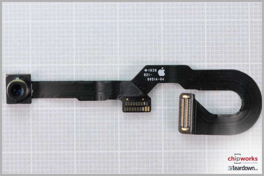
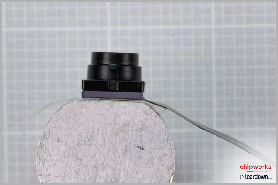
FaceTime Camera
FaceTime Camera
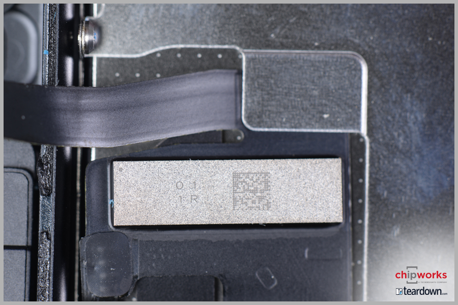
Touch Screen Controller
Touch Screen Controller
The Touch Controller for the iPhone 7 is manufactured by Universal Scientific Industries (USI) with markings O1 1R. It is the same as the iPhone 6S - a pressure-sensitive 3D Touch layer that buzzes slightly when you press and hold the screen/static home button. It was found under a metal shielding and though no markings were found on the IC, it is believed to be Analog Devices.
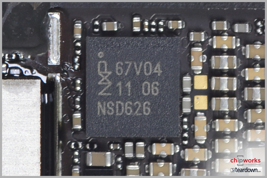
NFC Controller
NFC Controller
We found an NXP NFC Controller with package markings 67V04 (likely PN67V) in the iPhone 7. We will decap it to get the die photo to see if it is a new designed NFC controller. For your reference, the previous iPhone 6S had the NXP PN66V10 NFC Controller, which has the die PN549. TechInsights has done a circuit analysis report of the NXP PN549.
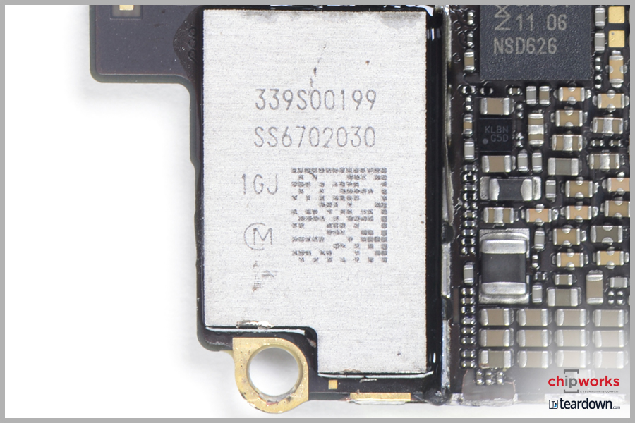
Wi-Fi
Wi-Fi
The WiFi / Bluetooth socket has been won by Murata with a module part number 339S00199. These modules have historically been multi-component packages. We will decap it to find who wins the Wi-Fi controller and verify who else might be within the module.
GPS
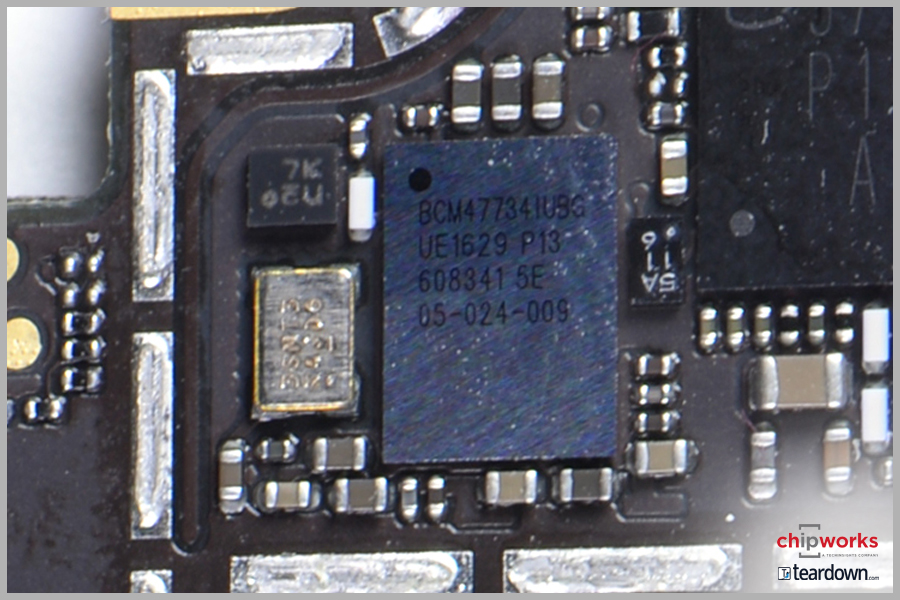
GPS
Broadcom wins the slot in the iPhone 7: BCM47734. This possibly contains Sensor Hub functionality as well like BCM4773 & BCM4774 seen in Samsung devices. Apple did announce the A10 has its own sensor hub, so if the BCM47734 does have a sensor hub it may not be utilized here in the iPhone 7.
Audio ICs
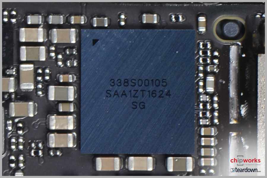
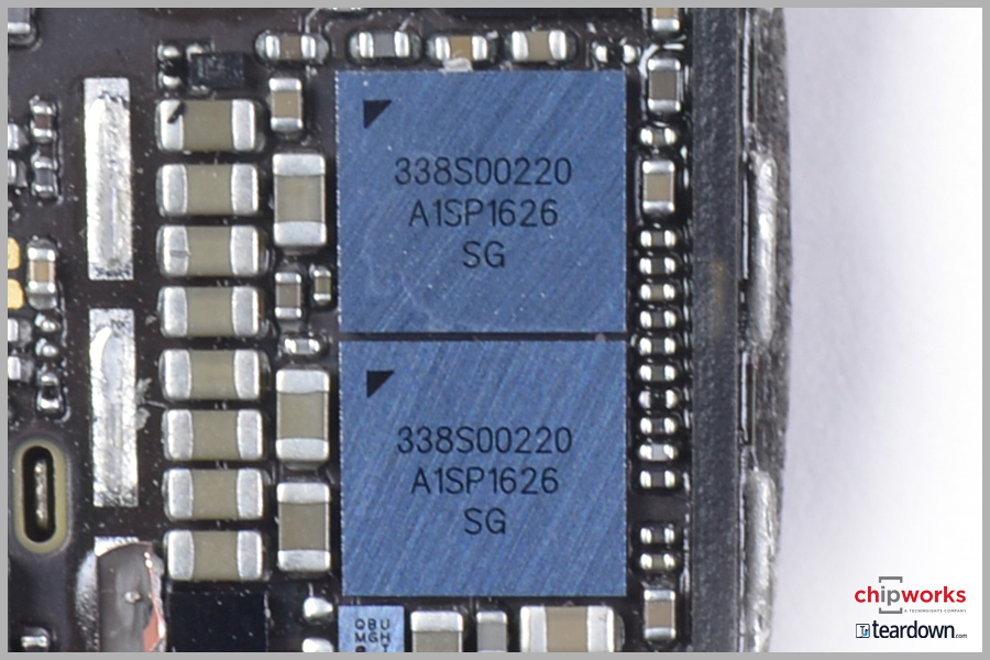
Audio ICs
The iPhone 7 still uses the same Apple/Cirrus Logic 338S00105 Audio Codec as in the iPhone 6S, but the Audio Amplifier has changed to the new 338S00220. (previously 338S1285 )
We found not just 2 but 3 Audio Amplifiers - we speculate there is one audio amplifier for for each of the two speakers, and the third amplifier is for the headphone via the Lightning port.
The third Audio amplifier is situated next to the Applications Processor Module with 3 black blobs on it. It was discovered during de-soldering of the A10 applications processor. When the blob was scraped off, it was an ‘oh wow, there are 3 audio amps!’ kind of discovery.
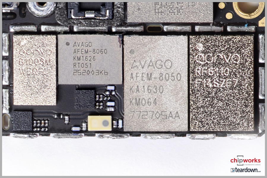
RF Front-end
RF Front-end
This time around (or at least in this version), Apple opted to use Skyworks for their GSM PA only, but not for any of the Low, Mid, or High band PA Modules. Those were covered by Avago (Broadcom) and Qorvo. Qorvo parts are now beginning to be marked Qorvo now rather than TriQuint or RFMD. Skyworks wasn’t left out though, and seemed to push out Murata for some of the Diversity Receive Modules used at the top end of the phone (although Murata did get the WiFi/BT Module socket). TDK-EPC has been making a single appearance in the last couple of iPhones and iPads, while this time we find what looks like to be filter bank sockets located centrally between the two Intel RF transceivers. The following table highlights the RF design wins.
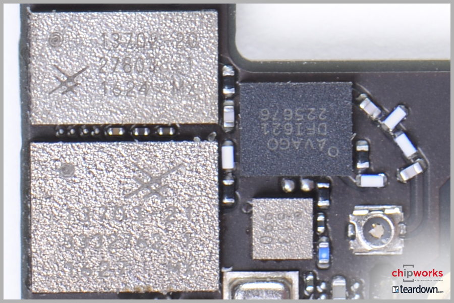
| Avago (Broadcom) | AFEM-8060 | Likely High-Band PAM (FBAR-BAW) |
| Avago (Broadcom) | AFEM-8060 | Likely High-Band PAM (FBAR-BAW) |
| Avago (Broadcom) | AFEM-8050 | Likely Mid-Band PAM |
| Qorvo | RF6110 | Likely Low-Band PAM |
| Qorvo | 81003M | Envelope Tracking Power Management IC |
| Skyworks | SKY77359 | GSM PA |
| TDK-EPC | D5313 | Filter Banks |
| TDK-EPC | D5325 | Filter Banks |
| Skyworks | SKY13702-20 | Diversity Receive Modules (integrated antenna switches) |
| Skyworks | SKY13703-21 | Diversity Receive Modules (integrated antenna switches) |
| Avago (Broadcom) | DFI621 | PA Duplexer Module |
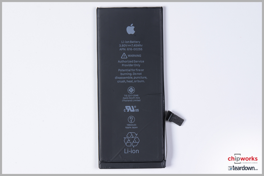
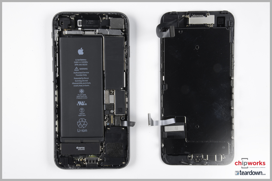
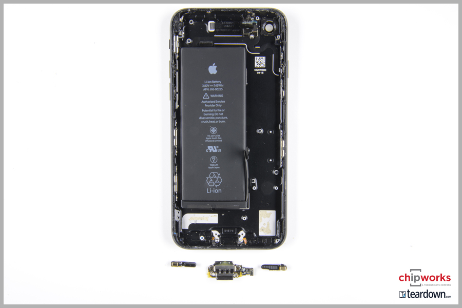
Battery
Battery
The battery is a 1960 mAh, 3.8 V (7.45 Wh) unit, credited with giving another two hours of performance compared with the 6-series - that had a slightly smaller power supply at 1810 mAh, 6.9 Wh. For comparison, the exploding batteries in the Samsung Galaxy Note 7 are 15.4 Wh and twice the size.
Other ICs
In the “miscellaneous” section we have:
- Lattice Semiconductor FPGA ICE5LP4K;
- NXP Interface IC 610A3B (likely a variant of CBTL1610A3);
- Texas Instruments Display Power Management TPS65730;
- Texas Instruments Battery Charger SN2400AB0;
- SiTime* MEMS Oscillator SiT1532;
- Alps Compass HSCDTD00xA;
- Bosch Sensortec Pressure Sensor (likely BMP282)