Posted: January 22, 2019
Contributing Author: Sinjin Dixon-Warren, PhD
TechInsights’ full analysis of the STMicroelectronics BCD9S referenced in this post is included in our new Power Semiconductor subscription, which addresses new technologies in the power semiconductor market, including GaN, SiC, plus Si MOSFET and IGBT devices.
TechInsights has been monitoring the evolution of STMicroelectronics Bipolar-CMOS-DMOS (BCD) technology for more than fifteen years, beginning in the year 2000 when we performed a structural and electrical characterization of a 0.8 µm BCD device with a 1999 mask date [1]. A few years later, in 2004, we analyzed the STMicroelectronics L6262S (VCM/Motor Controller) BCD integrated circuit, which had a 1998 mask date and 0.9 µm gate lengths [2]. The L6262S, shown in Figure 1, featured blocks of DMOS transistors along the edges of the die.
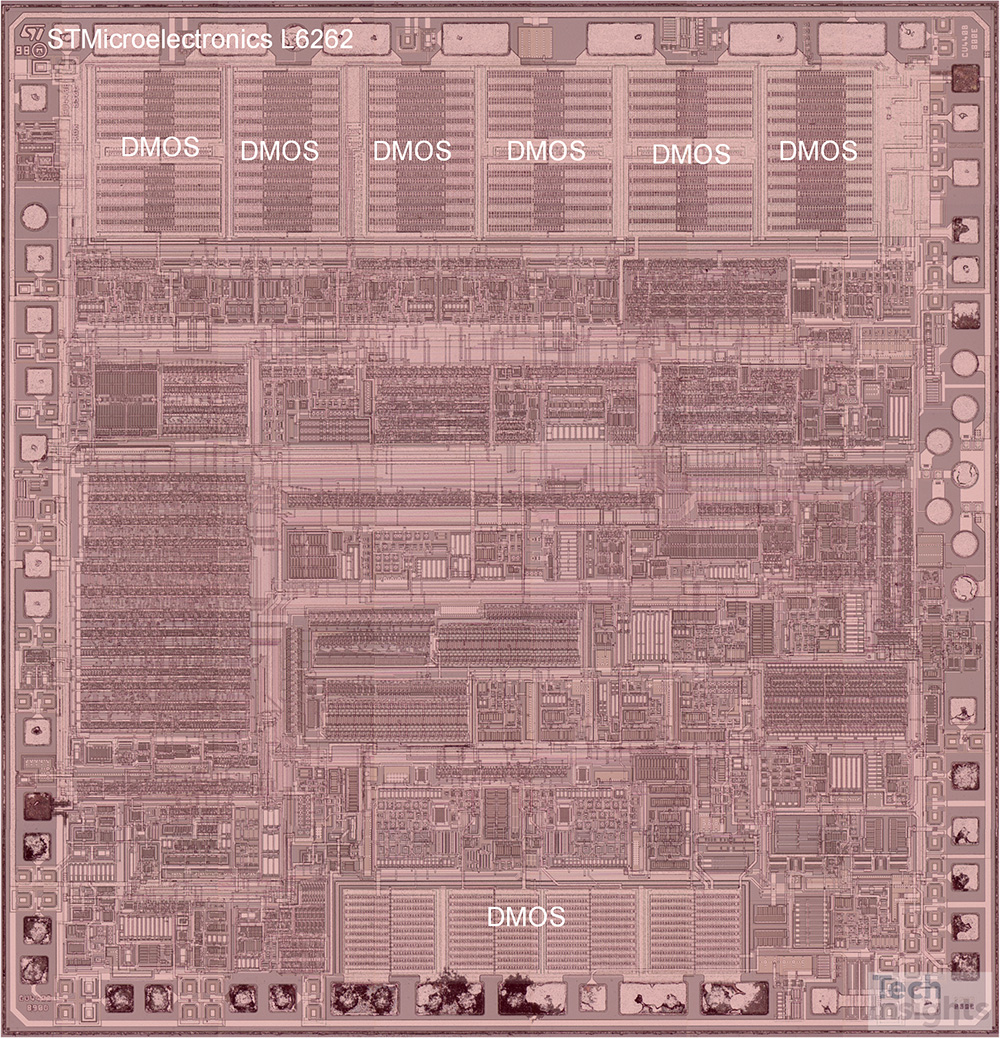
Figure 1 – STMicroelectronics L6262S BCD Process Die Photograph
BCD technology integrates CMOS logic, double diffused MOS transistors (DMOS), lateral diffused MOS transistors (LDMOS) and bipolar transistors into a single silicon die. The DMOS and LDMOS transistors are generally used to create high voltage or higher power output driver transistors, while the bipolar transistors provide analog functionality. STMicroelectronics is a market leader in BCD technology, which they claim to have invented in the mid-1980s [3]. The technology is also offered by other vendors, including Texas Instruments, Infineon, Atmel, Maxim and by major foundries, such as TSMC. TechInsights has reports on many of these competing technologies. Figure 2 shows a cross-section of the DMOS transistors found on the STMicroelectronics L6262S die.
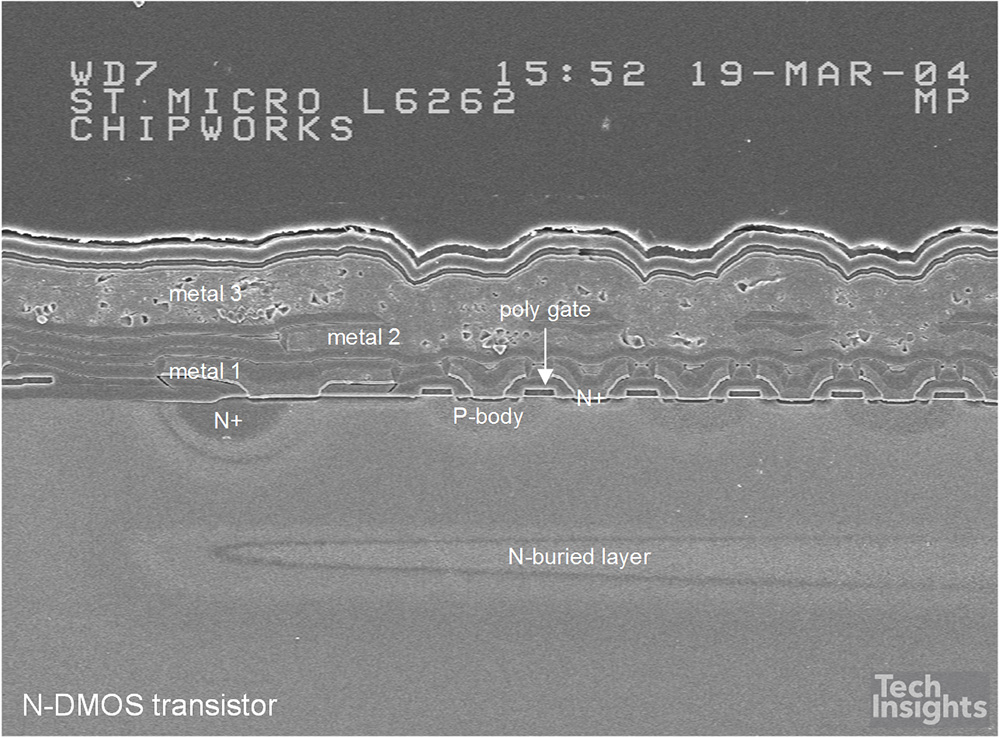
Figure 2 – STMicroelectronics L6262S N-DMOS Transistors
STMicroelectronics now offers three main BCD technologies, denoted BCD6, BCD8 and BCD9, corresponding to 0.32 µm, 0.16 µm and 0.11 µm technology, as shown in Figure 3. They claim to have a 90 nm BCD10 technology in development [4]. They have regularly published papers on these technologies at the International Symposium on Power Semiconductor Devices (ISPSD) conferences. TechInsights has reports on various specific versions of these STMicroelectronics BCD technologies [1, 2, 5, 6, 7, 8, 9]
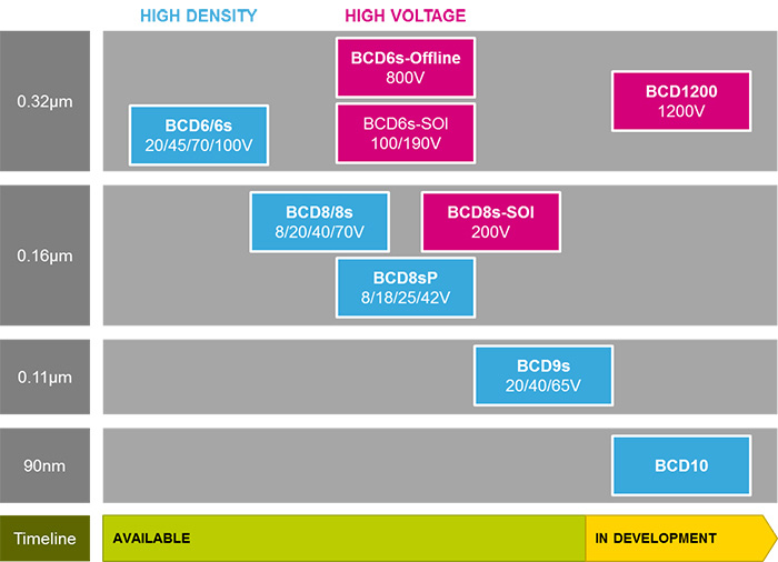
Figure 3 – STMicroelectronics BCD Technologies (source: STMicroelectronics)
Recently, TechInsights procures samples of the STMicroelectronics FDA801B-VYY 4x50 W class-D digital input power amplifier with I2C diagnostics, digital impedance meter and low voltage operation [10] which is fabricated with the new BCD9s technology [11]. A photograph of the FDA801B-VYY BCD9s die, deprocessed to diffusion, is shown in Figure 4. The die features blocks of analog, logic and LDMOS power transistors. We completed some preliminary analysis and have compared our findings with our previous analysis of STMicroelectronics BCD technologies.
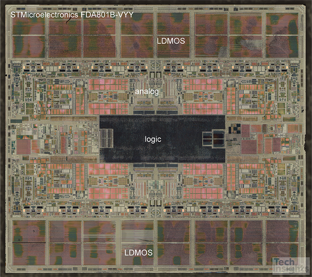
Figure 4 – STMicroelectronics FDA801B-VYY BCD9s Process Diffusion Die Photograph
Table 1 presents a summary of TechInsights process analysis findings for the series of different STMicroelectronics BCD technologies. In parallel with the rest of the semiconductor industry the trend has been towards smaller feature sizes, starting at about 1 µm for the BCD technologies in production around the year 2000. These early technologies featured DMOS transistors.
The BCD6 technology was released in about the year 2006 and featured 0.35 µm CMOS gates with three layers of aluminum metal planarized by chemical mechanical polishing (CMP). Figure 5 shows a photograph of the STMicroelectronics ST1S03 BCD6 die. A large DMOS switch transistor is found on the die. LDMOS transistors and NPN bipolar transistors were found and Local oxidization of silicon (LOCOS) isolation is used. Figure 6 shows a cross section of a typical LDMOS transistor found on the ST1S03 BCD6 die. The key characteristic of the LDMOS transistors is the presence of isolation and a drift region between the transistor gate and the drain contact. The gate extends over the isolation. These features allow the LDMOS transistor to support higher voltage bias between the source, which is at ground, and drain. Generally, a doped drift region extends beneath the gate resulting in a transistor channel which is shorter than the physical gate length. LDMOS transistors are challenging to design and manufacture, due to the large number of additional masks and implants required, as compared to standard CMOS technology.
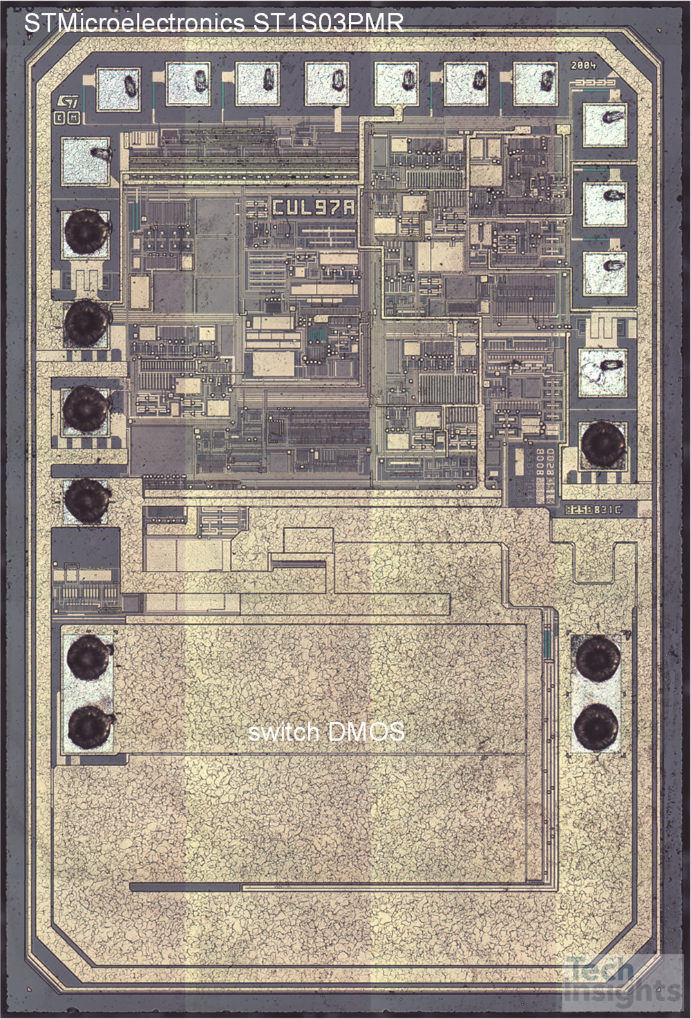
Figure 5 – STMicroelectronics ST1S03 BCD6 Process Die Photograph
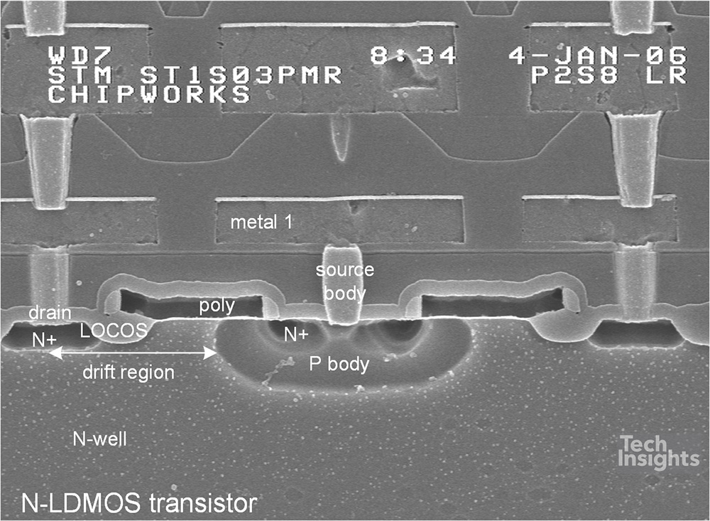
Figure 6 – STMicroelectronics ST1S03 N-LDMOS Transistors
The BCD8 technology was first released in about 2011. It featured 0.18 µm CMOS gates and four layers of CMP planarized Al metal, plus two layers of polysilicon with cobalt silicide, and shallow trench isolation (STI). Both N and P-type LDMOS transistors were found, plus bipolar transistors, poly-poly capacitors and 6T-SRAM memory. Figure 7 presents a photograph of the STMicroelectronics ST7570 BCD8 die. Complementary LDMOS transistors are located at the upper right corner. An example of the LDMOS transistors found on the ST7570 BCD8 die are shown in cross section in Figure 8. As can be seen in Figure 3 a high voltage silicon-on-insulator (SOI) version of the BCD8 technology is now also available, but has not yet been seen by TechInsights.
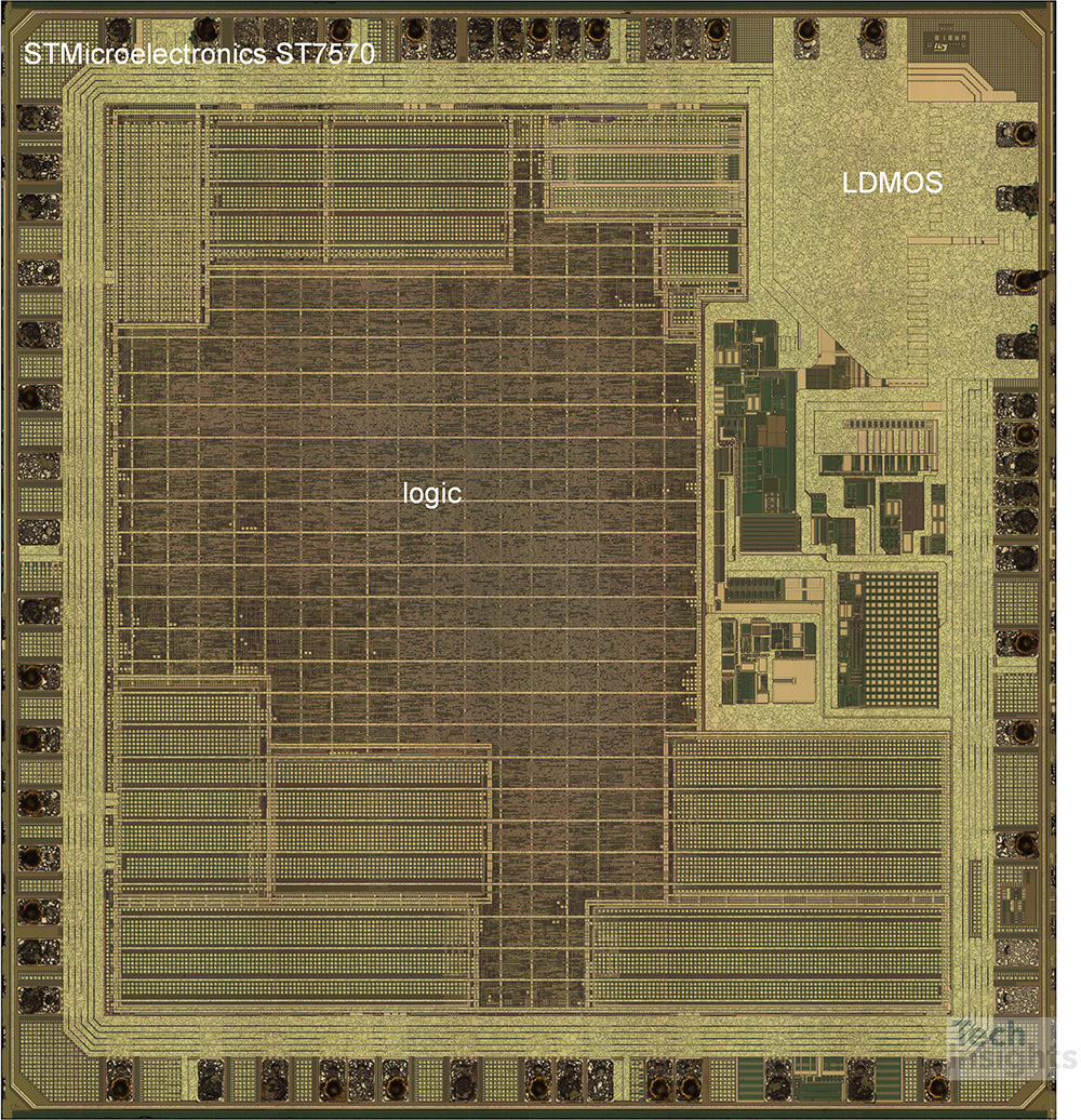
Figure 7 – STMicroelectronics ST7570 BCD8 Die Photograph
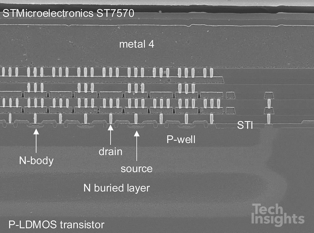
Figure 8 – STMicroelectronics ST7570 P-LDMOS Transistors
The 0.13 µm BCD9 process was released to the market in 2015. The technology features copper metallization and integrated the now extensive array of BCD features, including N and P-type LDMOS transistors, MIM capacitors, 6T-SRAM and bipolar transistors. A photograph of the STMicroelectronics FSB2D48 BCD9 die is shown in Figure 9, while Figure 10 shows an example of the N-LDMOS transistor layout found on the FSB2D48 BCD9 die.
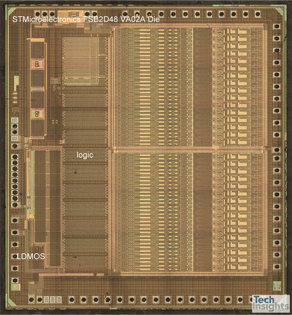
Figure 9 – STMicroelectronics FSB2D48 BCD9 Die Photograph
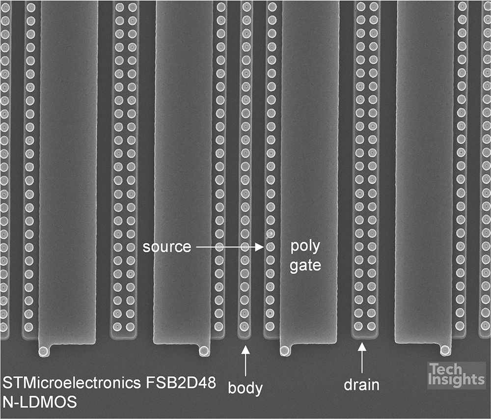
Figure 10 – STMicroelectronics FSB2D48 N-LDMOS Layout
In 2015 ST announced the BCD9s technology [11] as the second generation of their BCD9 0.13 µm process technology. Our preliminary analysis finds several key new features, including the addition of a thick top redistribution layer (RDL). The observed minimum contacted gate pitch for the logic transistors was 0.6 µm suggesting 0.13 µm process, rather than the 0.11 µm claimed by ST for the BCD9s. The technology now integrates three types of isolation. Deep trench isolation (DTI) is used to provide isolation between the various blocks of circuitry, the CMOS logic uses STI and LDMOS power transistor blocks use LOCOS isolation. This is the first time that TechInsights has seen all three types of isolation used on a single die. Figure 11 presents a cross section view of the STMicroelectronics FDA801B-VYY BCD9s process die edge, which shows the DTI and the RDL features. TechInsights is planning further analysis of the BCD9s technology, which will be available in an upcoming report.
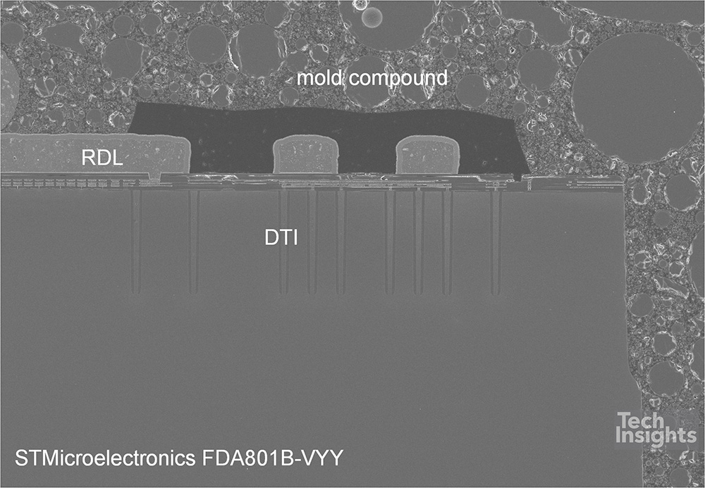
Figure 11 – STMicroelectronics FDA801B-VYY BCD9s Process Die Edge
BCD technology continues to be an area of active innovation in the power electronics market space. Unlike advanced CMOS, where the challenges are around the integration of the maximum number of MOS transistors into a given area, hence the relentless drive to smaller feature sizes, BCD technology is driven by the need to integrate a wide variety of different active devices onto a single die. This requires careful balancing of the disparate engineering needs of each device type.
Table 1 – STMicroelectronic BCD Technology Process Summary
| CUD16A BCD 0500-4376-FS43 |
L6262S BCD SAR-0408-008 |
ST1S03 BCD6 PPR-0601-801 |
ST7570 BCD8 PPR-1101-801 |
L6390DTR BCD OFF-LINE PPR-1301-803 |
FSB2D48 BCD9 PPR-1501-801 |
FDA801B-VYY BCD9S PPR-1803-801 |
|
|---|---|---|---|---|---|---|---|
| Year | 2000 | 2004 | 2006 | 2011 | 2013 | 2015 | 2018 |
| Mask Date | 1999 | 1998 | 2004 | 2009 | 1998 | 2012 | 2014 |
| Generation | 1 µm | 1 µm | 0.35 µm | 0.18 µm | 3 µm | 0.13 µm | 0.11 µm (claimed) |
| Number of Metals | 3 | 3 | 3 | 4 | 1 | 5 | 3 |
| Number of polys | 2 | 2 | 1 | 2 | 2 | 1 | 1 |
| Silicide | WSi | - | TiSi | CoSi | - | CoSi | CoSi |
| RDL | No | No | No | No | No | No | Yes |
| Metal Type | Al | Al | Al | Al | Al | 4 Cu, 1 Al | Cu |
| Contacts | W | Al | W | W | Al | W | W |
| Vias | W | Al | W | W | - | Cu | Cu |
| CMP | No | No | Yes | Yes | No | Yes | Yes |
| Isolation | LOCOS | LOCOS | LOCOS | STI | LOCOS | STI | LOCOS STI DTI |
| Power transistors | DMOS | DMOS | LDMOS with LOCOS | LDMOS with STI | LDMOS with LOCOS | LDMOS with STI | LDMOS with LOCOS |
| Bipolar transistors | NPN | NPN and PNP | NPN | NPN | NPN | NPN and PNP | NPN |
| Passives | Resistors | Resistors, poly capacitors and diodes | Resistors, poly capacitors and diodes | Resistors and poly-poly capacitors | Resistors and poly-poly capacitors | MIM capacitors and resistors | Capacitors and resistors |
| SRAM | No | No | No | ST-SRAM | No | 6T-SRAM | Yes |
TechInsights’ full analysis of the STMicroelectronics BCD9S referenced in this post is included in our new Power Semiconductor subscription.
The purpose of this subscription is to provide access to our analysis of new technologies in the power semiconductor market, including GaN, SiC, plus Si MOSFET and IGBT devices. It also includes our library of BCD technology reports.
Learn more about the TechInsights Power Semiconductor subscription.
- A Structural Analysis of the BCD Transistors (Bipolar, CMOS, DMOS), Including Electrical Characteristics, of an STMicroelectronics Microcontroller, Report ID#: 0500-4376-FS43, TechInsights, May 26, 2000.
- STMicroelectronics L6262S BCD-MOS IC Process Review, PPR-0408-008, TechInsights, August 31, 2004.
- http://cmp.imag.fr/IMG/pdf/bcd8s-soi_technology_overview-2.pdf
- http://www.st.com/content/st_com/en/about/innovation---technology/BCD.html
- STMicroelectronics ST1S03 BCD6 LDMOS Process Review, PPR-0601-801, TechInsights, January 16, 2006.
- STMicroelectronics ST7570 180 nm BCD8 - Process Analysis Report, TechInsights, TechInsights, PPR-1101-801, July 1, 2011.
- STMicroelectronics ST7570 N-LDMOS and P-LDMOS BCD Electrical Characterization Report, TechInsights, CWR-1103-906, March 3, 2011.
- STMicroelectronics L6390DTR High-Voltage High/Low-Side Driver BCD OFF-LINE Process Review, TechInsights, PPR-1301-803, August 1, 2013.
- STMicroelectronics FSB2D48 BCD9 Process Review Report, TechInsights, PPR-1501-801, January 1, 2015
- http://www.st.com/en/automotive-infotainment-and-telematics/fda801b.html
- http://www.st.com/content/st_com/en/about/media-center/press-item.html/p3767.html


