The chips behind AI aren't shrinking. They're stacking.
Get the Roadmap: Advanced Packaging Technology and Market Analysis Report.
It's a lab-backed guide to the technologies, foundry and OSAT roadmaps, and market shifts redefining compute performance. Register for the TechInsights Platform to access the full report.
The industry is no longer solving performance with a single larger die.
Chiplets, 2.5D and 3D stacking, hybrid bonding, and HBM are now the architecture decisions shaping AI and HPC silicon.
How advanced packaging became the engine of the AI and HPC era
For decades, better chips meant smaller transistors. Now AI and high-performance workloads demand more compute than any single die can deliver, so the action has moved into the package. Advanced packaging now shapes performance, power efficiency, form factor, and system integration. It has become one of the primary drivers of semiconductor innovation.
Our advanced packaging reports give you a clear, data-backed view of that landscape: where it stands today, how the major players compare, and where it's headed next.
What You'll Get
A shared foundation
Clear definitions of the concepts, architectures, and industry dynamics behind advanced packaging, so technical and commercial teams work from the same understanding.
Technology scaling trends
How packaging technologies are scaling, and what's driving the shift from monolithic dies to multi-die integration.
Technology positioning
How the leading packaging approaches compare, and where each is positioned in the market.
Foundry and OSAT roadmaps in one place
Consolidated data on leading-edge packaging offerings from today's major wafer foundries and top OSATs, and how each provider's capabilities shape the broader market.
Evidence, not vendor claims
Every technology comparison draws on TechInsights' lab-based analysis of real-world devices, so the insight rests on actual silicon rather than marketing.
Advanced packaging is where compute performance is now won. See the roadmap and more reports we think you’ll like.
Register for the Platform to explore the analysis behind today's most important packaging transitions.
Create your free account and start exploring today.
Corporate email required. Takes under a minute.
By submitting this form, you consent and agree to the creation of a TechInsights Platform account and agree to the terms of the End User License Agreement and Privacy Policy. You will also receive communications related to your account and the related report recommendations.
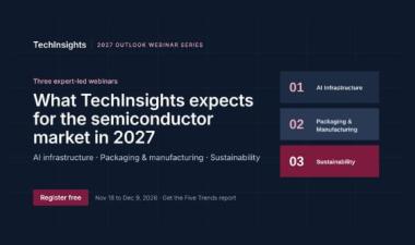
2027 Outlook Webinar Series: AI, Packaging, Manufacturing & Sustainability
Register for three 2027 outlook webinars. Get the free Five Trends report now, plus every 2027 Outlook report as it publishes in the TechInsights Platform.

TechInsights Outlook 2027: Five Trends Reshaping the Market
Explore five trends shaping the 2027 semiconductor market, from memory constraints and AI infrastructure to advanced packaging, emissions and consumer demand.

Apple A20 Pro: Inside the iPhone 18 Pro’s TSMC 2nm Processor
TechInsights analyzes Apple’s A20 Pro processor, revealing TSMC N2 gate-all-around technology, expanded AI and graphics processing, and a new side-by-side memory packaging architecture.

The Authoritative Information Platform to the Semiconductor Industry.