Latest Image Sensor Insights & Analysis
OmniVision OV50K Device Essentials Folder
This report provides an overview into the structure of the OmniVision OV50K CIS. The analysis provides foundry identification and details of the fabrication process used to manufacture the image sensor and image signal processor (ISP) and a summary of the salient features observed, and is accompanied by a set of optical, SEM cross-section, and bevel images of both CIS and ISP dies.Omnivision OX08D10 Standard Floorplan Analysis
This report provides an insight into the structure of the OmniVision OX08D10 CMOS image sensor ISP die for automotive applications. The analysis provides foundry identification and a summary of the salient features observed that is accompanied by a set of SEM cross-section of the ISP die.Omnivision OX08D10 Device Essentials Folder
This report provides an overview into the structure of the OmniVision OX08D10 CMOS image sensor (CIS). The analysis provides foundry identification and details of the fabrication process used to manufacture the image sensor and image signal processor (ISP) and a summary of the salient features observed, and is accompanied by a set of optical, SEM cross-section, and bevel images of both CIS and ISP dies.
2024 Image Sensor - Image Signal Processor Video Briefing 1
In this briefing, foundries and process nodes used to fabricate the devices are identified, and floorplan and layout are discussed including the area allocated to the analog to digital converters, digital processing, and embedded SRAM.
Prophesee GenX320 Process Flow Analysis
Prophesee GenX320 Process Flow Analysis

Sony A9 III Digital Camera Sensor (IMX810AQL) Device Essentials Folder
Sony A9 III Digital Camera Sensor (IMX810AQL) Device Essentials Folder

Google I/O 2026: Gemini for Home Takes Center Stage
Google I/O 2026 focused on Gemini for Home, AI-powered smart devices, and agentic AI, signaling a software-first future for the smart home market.
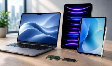
PC and Tablet Market Trends | AI PCs, Apple M5 & Memory Costs
Discover the latest PC and tablet market trends, including AI PCs, Apple M5 devices, Intel Panther Lake, processor forecasts, tablet market share, and the impact of rising memory costs.
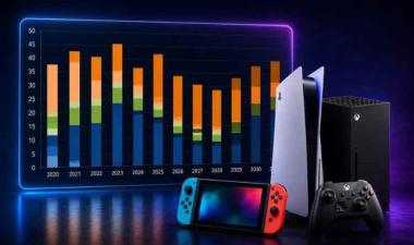
Game Console Forecast 2030: Rising Prices, Declining Shipments, and the Future of Gaming
Discover why rising memory costs, higher console prices, and longer upgrade cycles are expected to slow game console shipments through 2030. Explore the outlook for Nintendo Switch 2, PlayStation, and Xbox in the latest TechInsights forecast.