contributed by Dr. Sinjin Dixon-Warren
TSMC’s 28 nm CMOS technology platform is currently their most advanced offering. Our analysis suggests that this will be a very profitable technology platform for TSMC and for their fabless design partners for many years to come. In fact, Chairman Morris Chang expects that 28 nm will be the biggest node ever, exceeding the 65 nm node in production volumes, with more than 130,000 wafers per month at the peak.
Historically, TSMC was used to a slower ramp with leading customers such as FPGA vendors Altera or Xilinx; with 28 nm the ramp included Qualcomm and other mobile-driven companies, and demand switched on much more quickly. So while in the first quarter this year 28-nm was about 5% of sales, in the last quarter it is expected to be more than 20%.
At SEMATECH’s 9th International Symposium of Advanced Gate Stack Technology in Saratoga NY Meikei Ieonge of TSMC presented at nice overview of the TSMC’s 28 nm offering (some details can be found in a previous blog posting). The TSMC 28 nm technology is offered in four versions and is now shipping in volume for a variety of manufacturers, including Xilinx, Altera, AMD, Qualcomm and others.
TSMC was founded in 1987 and is the world’s largest foundry with 2011 revenues reaching $14.5 billion. According to their web site their total manufacturing capacity in 2011 was 13.2 million eight-inch wafer equivalents. They presently offer the full range of CMOS technologies from >0.5 µm down to 28 nm.
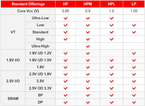
The 28 nm technology platform appeared in production in 2010 and is offered in four process variants, denoted HP, HPM, HPL and LP. We have analyzed three of these process variants to date, namely HP, HPL and LP. The 28 nm generation was the first time TSMC used high-k metal gate (HKMG) transistors. The HP and HPL technologies feature HKMG transistors, while the LP uses conventional poly gates, with an ONO gate dielectric. TSMC claims that their 28 nm process technology entered production in 2010; however, production devices were not available for analysis until mid-2011.
The early adopters of TSMC’s most advanced process technologies continue to include Xilinx and Altera, the two leading FPGA manufacturers. These companies make high value, relatively low volume devices, and thus can afford the relatively low yields seen in the early ramp of a new CMOS technology. It should be no surprise that often the first devices at a new technology node to hit our labs come from these vendors; and it has been thus since our analysis of the 130 nm Altera Stratix in 2002 and the 90 nm Altera Stratix II in 2004. Back then, the Altera Stratix feature cobalt silicided poly transistors with a 530 nm contacted gate pitch, while the transistors in the Stratix II had a 370 nm contacted gate pitch.
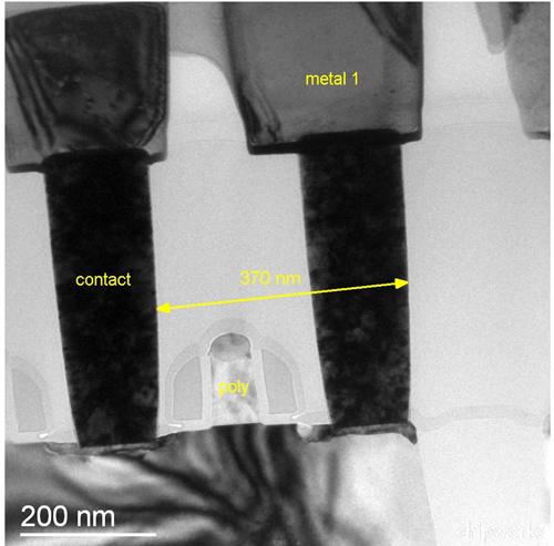
Altera Stratix II 90 nm Transistor – TEM
The Xilinx XC7K325T Kintex-7 was the first 28 nm TSMC technology seen by our labs. We published our Structural Analysis Report in July of 2011. The XC7K325T was built using TSMC’s HPL technology, and featured 11 layers of backend metallization. The HKMG transistors had the channel direction rotated to the <100> orientation to increase the performance of the PMOS transistors. Embedded SiGe was not used for the PMOS source/drains. The transistor metallurgy was quite similar to that seen for the Intel 32 nm technology, with a TiN metal gate for the PMOS and a TiAlN metal gate for the NMOS. Hafnium oxide based dielectric was used for the HK layer, over a 2.0 nm thick layer of silicon dioxide. The transistors are formed by a poly gate replacement, “gate last” process, similar to that used by Intel. Essentially, poly transistors are formed and all the source/drain engineering is completed. The poly is then removed and is replaced with NMOS and PMOS metallization. The contacted gate pitch for the transistors in the XC7K325T is 120 nm. According to TSMC the HPL process is optimised for high performance with low leakage.
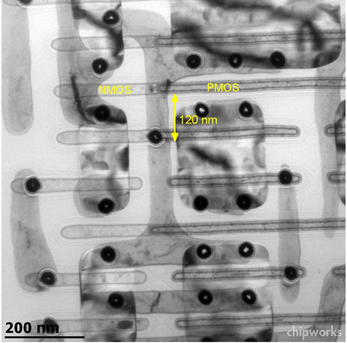
Xilinx XC7K325T Kintex-7 TSMC 28 nm HPL – Plan View TEM
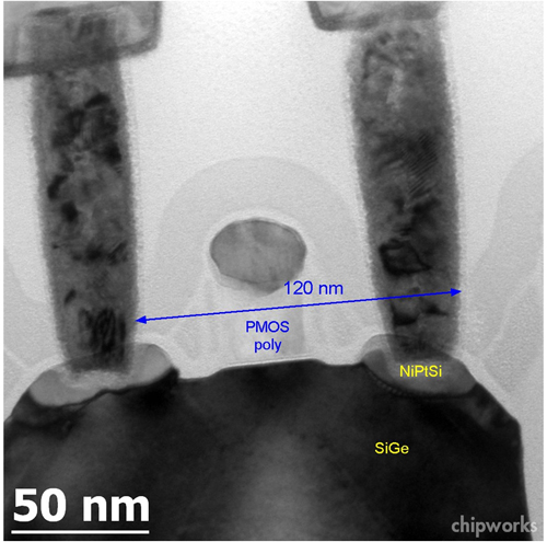
The Altera 5SGXEA7K2F40C2ES Stratix V was the second 28 nm TSMC technology to be analyzed our labs. Our Process Review Report was published in October of 2011. The Stratix V was fabricated with the 28 nm HP process, which features embedded SiGe in the source/drain regions of the PMOS transistors, and 12 layers of metal in the backend. The HKMG structure was essentially identical to that used in the HPL process, but with a thinner (1.2 nm) SiO2 layer, as befits an HP process. The contacted gate pitch for the 5SGXEA7K2F40C2ES transistors was 120 nm. According to TSMC, the 28 nm HP process is targeted for higher speed and performance, and they claim a 45% speed improvement when compared to the 40 nm process, with the same leakage per gate.
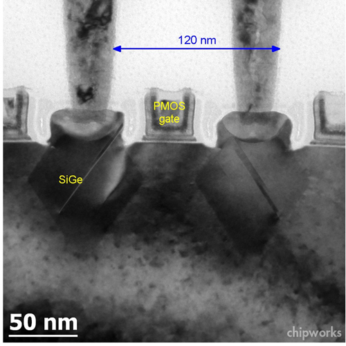
Altera 5SGXEA7K2F40C2 Stratix V 28 nm HP PMOS – TEM
The FPGA manufacturers do not make extensive use of high density SRAM in their chip designs. Here we look to AMD’s graphics division and nVidia – both early adopters of TSMC’s new process technologies. Their graphics processing chips incorporate large amounts of high density 6T-SRAM. We usually find that AMD/ATI or nVidia are the first chips to market using the full feature set of TSMC’s advanced technologies, including high density SRAM.
Earlier this year, we completed a limited analysis of the high density SRAM on the AMD RadeonTM HD 7970 215-0821060 graphics processor, which was fabricated with TSMC’s HP process. Our TEM analysis confirmed the 215-0821060 transistor structure was identical to that seen in the Altera Stratix V device, as would be expected since both are based on the TSMC 28 nm HP process. The 215-0821060 features a 0.16 µm2 6T-SRAM with the transistors arranged in a uniaxial layout. By contrast the 90 nm ATI 215PADAKA12FG graphics processor extracted from ATI Radeon X1950 Pro Graphics Card had a SRAM cell that is over five times bigger, at 0.86 µm2.
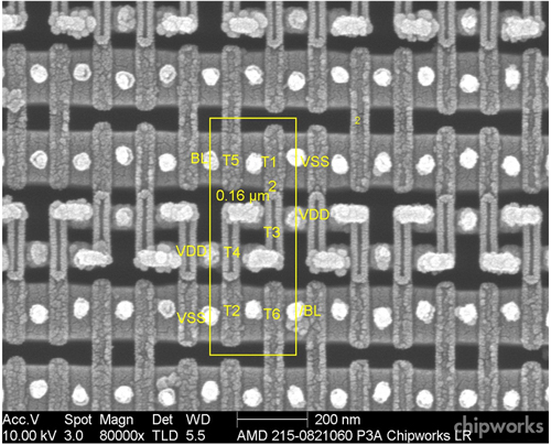
AMD 215-0821060 28 nm HP 6T-SRAM at Poly – Plan View SEM
Earlier in 2012, we found an example of TSMC 28 nm LP process in the Qualcomm MSM8960 Snapdragon S4 system-on-chip. The 28 nm LP process features polysilicon gates with embedded SiGe being used to increase the PMOS performance. The low power (LP) process was apparently the first available to have completed all TSMC’s qualification tests. TSMC claims that the 28 nm LP process is the low cost and fast time to market choice, ideal for low standby power applications such as cellular baseband. The process apparently provides a 20 percent speed improvement over the 40 nm LP process at the same leakage per gate.
The minimum contacted gate pitch was 120 nm. The 28 nm LP process is essentially a shrink of TSMC’s 40 nm LP process (with the addition of the e-SiGe for PMOS), which was (notably) used to fabricate the NVIDIA Tegra T20-H-A2 application processor. The 40 nm LP process featured a 160 nm contacted gate pitch in the logic regions.
Qualcomm MSM8960 28 nm LP Snapdragon S3 Transistor Gate – TEM
The fourth and final 28 nm process offered by TSMC is the HPM technology. This process is targeted at mobile applications and apparently will support both high performance transistors and low power transistors on the same die, thus enabling higher performance mobile devices, while continuing to improve power performance, which is critical in battery powered gadgets. TSMC claims the technology can provide better speed than 28 nm HP while giving similar leakage power to 28 nm LP. The wide performance/leakage coverage apparently makes 28 nm HPM ideal for applications from networking, tablet, to mobile consumer products. The HPM process has not yet been seen in the market yet, but Chipworks expects to see an example of the technology soon in a mobile device from a leading manufacture sometime soon – possibly a future variant of the Apple A6.


