Posted: April 7, 2017, Updated: April 25, 2017
We are excited to announce receipt of our Galaxy S8. Our blog details teardown findings including cost observations, verification of the 10 nm LPE process, commentary on the Qualcomm WTR5975 Gigabit LTE Transceiver and envelope tracking power supplies, information on rear and front facing cameras a list of design wins, and much more. We encourage you to scroll through to see all that we have uncovered.
Galaxy S8 Cost Observations
The 64 GB Samsung Galaxy S8 (SM-G950W) that we analyzed has a quick turn estimated Cost of Goods Sold (COGS) of $309.50. This being a quick turn is likely to be a little different from the estimate once we do our comprehensive deep dive teardown on it. By comparison, the 32 GB Samsung Galaxy S7 (SM-G930V) that we published in February 2017 has an estimated COGS of $243.00. If we normalize the memory to 64GB, this estimate jumps up to $257.00 using today’s NAND Flash numbers.
While the Samsung Galaxy S8 is a logical successor to the Galaxy S7, it is really more of an update to the failed Galaxy Note 7 that we also released at back in February 2017. Our published COGS estimate was approximately $270 using market value data at that time.
Cost Drivers:
This comparison will be mostly between the Galaxy S7 and Galaxy S8 with minor exceptions when necessary.
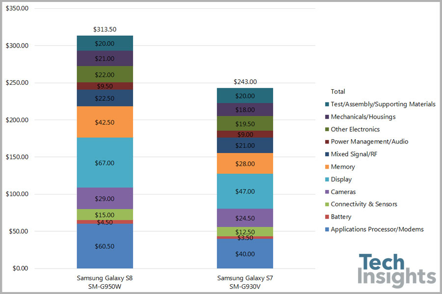
| Samsung Galaxy S8 SM-G950W | Samsung Galaxy S7 SM-G930V | |
|---|---|---|
| Applications Processor/Modems | $60.50 | $40.00 |
| Battery | $4.50 | $3.50 |
| Connectivity & Sensors | $15.00 | $12.50 |
| Cameras | $29.00 | $24.50 |
| Display | $67.00 | $47.00 |
| Memory | $42.50 | $28.00 |
| Mixed Signal/RF | $22.50 | $21.00 |
| Power Management/Audio | $9.50 | $9.00 |
| Other Electronics | $22.00 | $19.50 |
| Mechanicals/Housings | $21.00 | $18.00 |
| Test/Assembly/Supporting Materials | $20.00 | $20.00 |
| Total | $313.50 | $243.00 |
Applications/Baseband Processor: The Galaxy S7 was shipping using the Qualcomm Snapdragon 820 quad-core MSM8996 built on a 14nm process. This was a mature part, having first been seen about 15 months prior. Our latest cost estimate on it was approximately $40. When first observed, our cost estimate was approximately $57. This price erosion comes from the normal cost savings measures and margin compression. The Galaxy S8 is shipping with the new Qualcomm Snapdragon 835 octo-core MSM8998 built on a Samsung 10nm FinFET process. This being the first product in which we have observed it, has an estimate price of $60.50. It is significantly higher than the current estimate of the MSM8996, but only marginally higher than the launch price estimate.
Camera/Image: Both the Galaxy S7 and Galaxy S8 have comparable dual pixel OIS 12 megapixel rear cameras. The front camera on the Galaxy S8 was improved to 8 megapixels from the 5 megapixels on the Galaxy S7. Samsung also added an Iris scanner camera that was seen on the Note 7 that was not on the Galaxy S7. So, between the improved front camera and the addition of the Iris scanner camera, we are seeing a $5.50 jump in this category.
Connectivity: We are seeing a $2 jump in Connectivity mainly due to the new cutting-edge Murata Wifi/Bluetooth module. It is the first to employ Bluetooth 5.0 LE.
Display/Touchscreen: The new, 5.8”, 2960x1440 quad-pixel+ SuperAMOLED display is a beast. It adds 400 more rows of pixels in height (576,000 more pixels total) compared to Galaxy S7 and Galaxy Note 7. Like the Note 7, it is a dual edge display while the Galaxy S7 is flat. It also has a home key force touch sensor built in. Our quick turn estimate of this display is $67.00. This compares to the Note 7 at $55 and the Galaxy S7 at $47. The major cost factors when compared to the Note 7 are the additional pixels and quad pixel technology. The Galaxy S7 is really less of a comparison since it is smaller and has flat edges.
Memory: NAND Flash non-volatile memory experienced a significant jump in price during the first quarter of 2017. Due to the timing, this was not picked up in either the Galaxy S7 or Note 7 costs because it was just starting to make its upward movement. In the Galaxy S7, we saw a Samsung 32GB MLC NAND flash part at the time estimated to $7.50. If we change that to a 64GB Samsung MLC NAND part, we would currently be approximately $21. Now, the Galaxy S8 employs a Toshiba 64 GB part, which since it is not internally made, we estimate it to cost Samsung $24 to buy, hence the difference in non-volatile memory.
Volatile memory on the other hand has been on the decline since February, so we are expecting the 4GB LPDDR4X memory that Samsung is using in their Galaxy S8 to be a little cheaper than our estimate on the S7 a couple months back. In this case it went from approximately $20 to $18.50.
Non-Electronics: The major housings in the Galaxy S8 are more similar to the Note 7 and are on par with the Note 7 in terms of cost at $21. The Galaxy 7 has their parts at roughly $18 due to being smaller and manufactured differently.
RF Component: The Galaxy S7 employed two Qualcomm RF transceiver parts, the WTR3925 and the WTR4905. In the Galaxy S8, they only employed a WTR5975, but while the two parts in the Galaxy S7 added to about $5.50, the much larger die and higher functionality of the WTR5975 is about $2.50 more expensive at about $8.00!
Register to receive a complimentary teardown report on the Samsung Galaxy S8
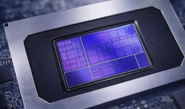
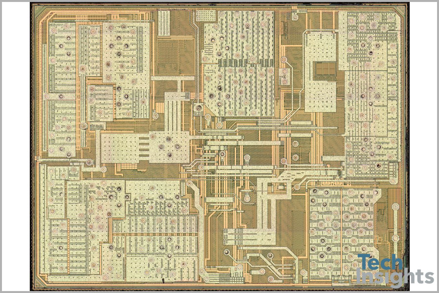
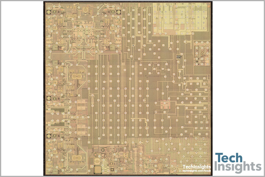
Qualcomm Snapdragon 835
Qualcomm Snapdragon 835
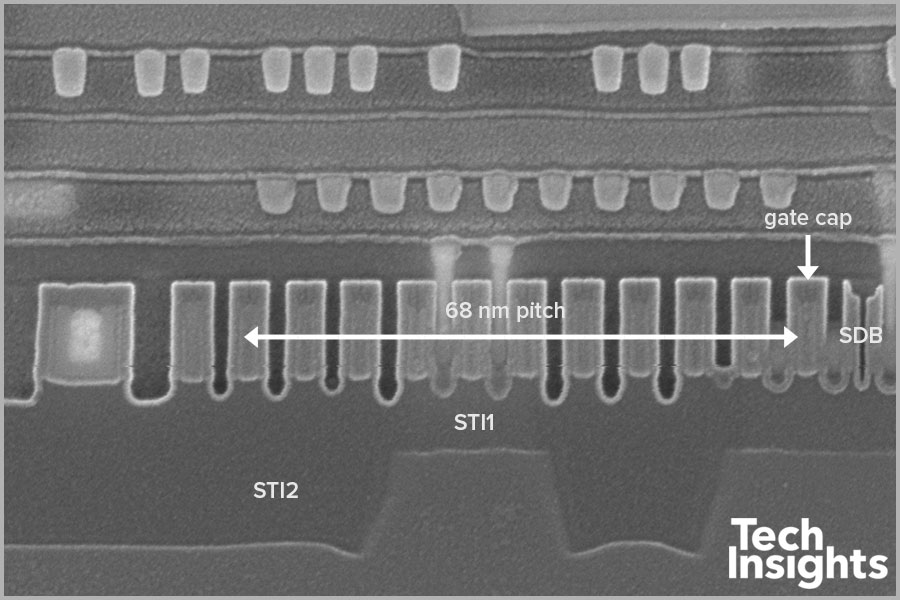
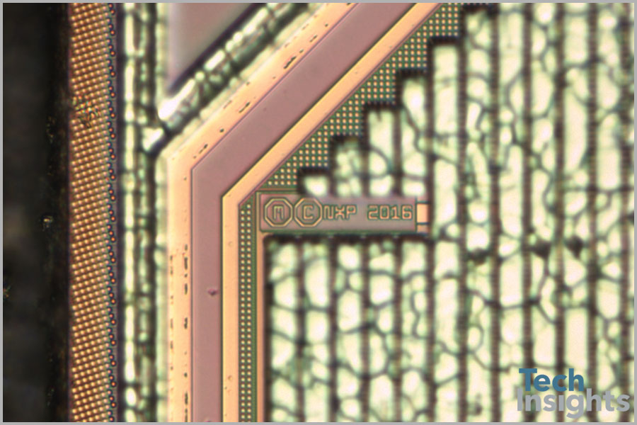
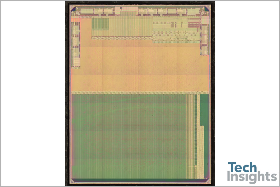
The Qualcomm Snapdragon 835 applications processor is confirmed to be built on Samsung’s 10 nm LPE process. We are able to confirm a 68 nm contacted gate pitch with dummy poly single diffusion break (SDB) capability. The minimum BEOL pitch is difficult to determine with a cross section, but we expect to find the publically published 48 nm pitch to be the minimum, once our functional block analysis looks into the specific layout features.
Overall, the process appears to be similar to Samsung’s 14LPE and 14LPP processes, with a dual shallow trench isolation (STI) and extra processing necessary to enable a dummy poly SDB. The contacts have been simplified to a single level to avoid a large increase in mask count. While the gate has a dielectric cap and appears to be self-aligned contact capable, the initial cross sections are not showing much, if any, usage of the gate cap.
Update! First to the 10 nm productization finish line is the Qualcomm Snapdragon 835, built on Samsung LSI Foundry’s 10 nm LPE technology. Check out more on our 10 nm blog.
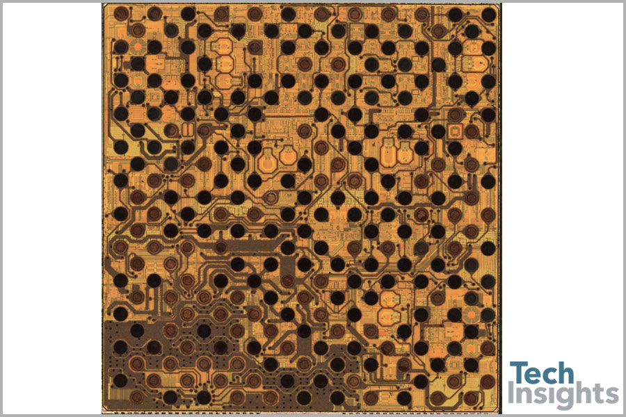
WTR5975 showing the redistribution layer (RDL)
Transceivers and Envelope Tracking Power Supplies
The S8 contained the first mobile phone design win we have seen for the new Qualcomm WTR5975 Gigabit LTE transceiver, as well as the new QET4100 envelope tracking power supply. We first observed the WTR5975 in a mobile LTE dongle.
The WTR5975 is a member of the Snapdragon 835 family. It is the world’s first single-chip RF IC supporting Gigabit Class LTE, LTE-U, and LAA with 5 GHz unlicensed band support. It supports up to 4x downlink CA, 2x uplink CA, all 3GPP-approved bands, including 3.5 GHz bands 42 and 43, and 4x4 MIMO in a single transceiver chip, dramatically reducing the footprint required to support advanced CA and MIMO configurations.
The WTR5975 is in our labs right now as we have been in full production extracting the circuit design on the transmit and receive paths. Now that we have the new QET4100, we will begin producing a full chip Circuit Analysis of this device as well. Please contact us for more information and a copy of our product brief on the WTR5975 and QET4100.
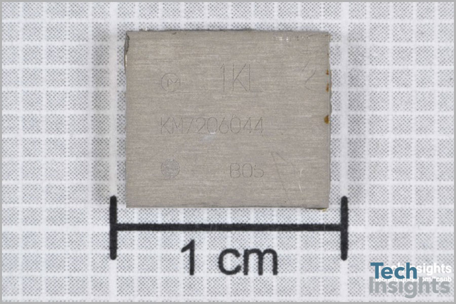
Wi-Fi/Bluetooth
Wi-Fi/Bluetooth
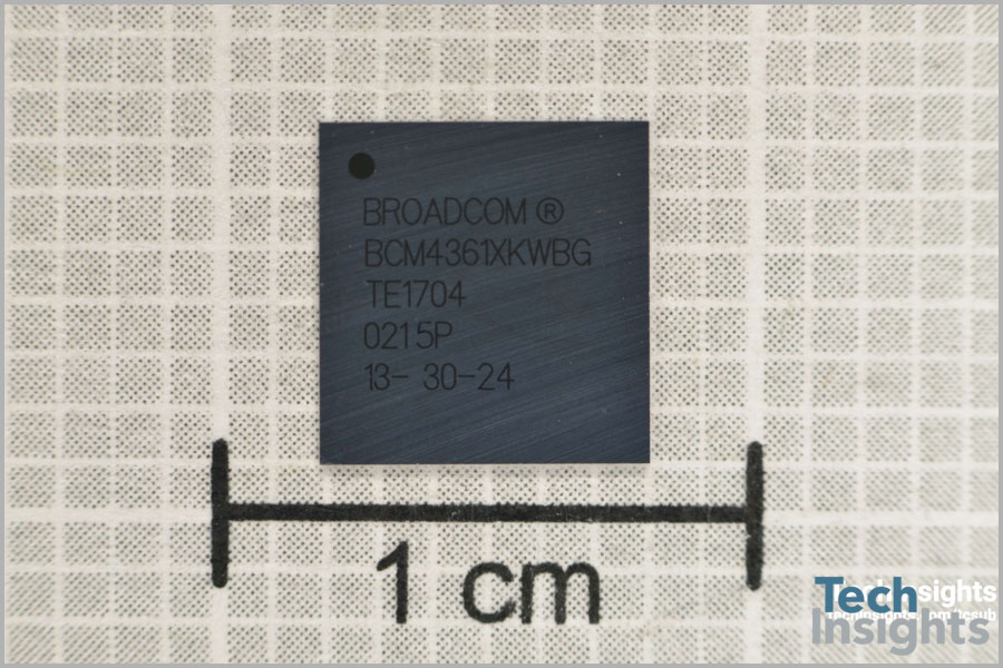
We have now decapped the Murata Wi-Fi module KM7206044. Inside, we found the Broadcom BCM4361 SoC and a few other dies. The BCM4361 is very likely a single-chip SoC with integrated Wi-Fi and Bluetooth 5.0.
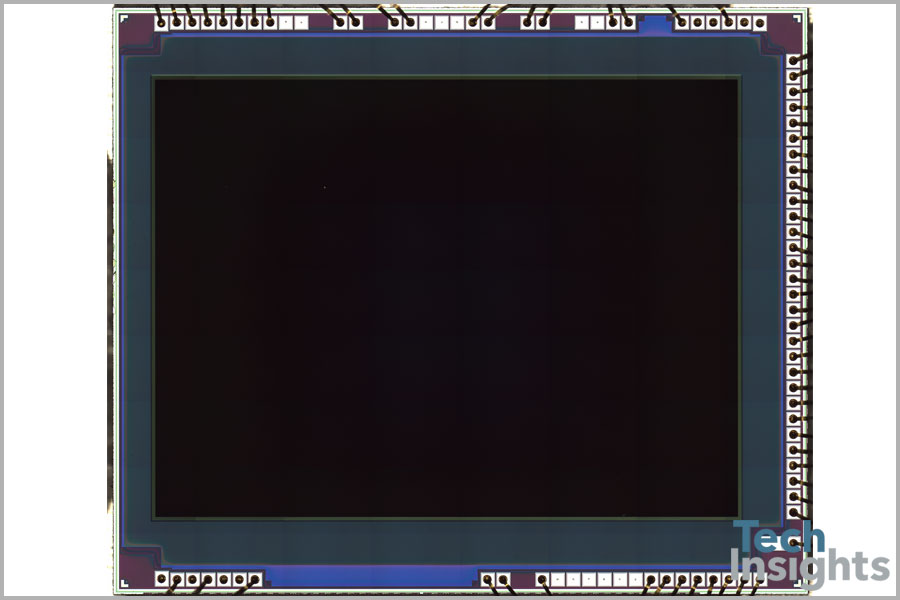
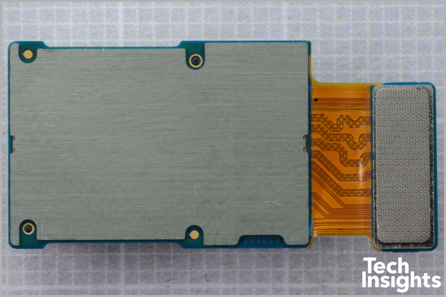
Front-Facing Camera
Front-Facing Camera
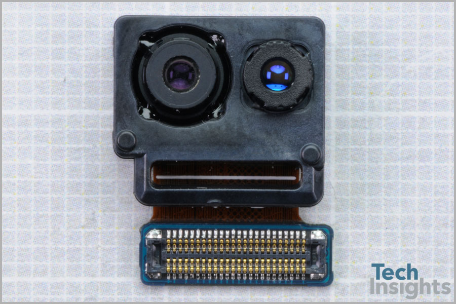
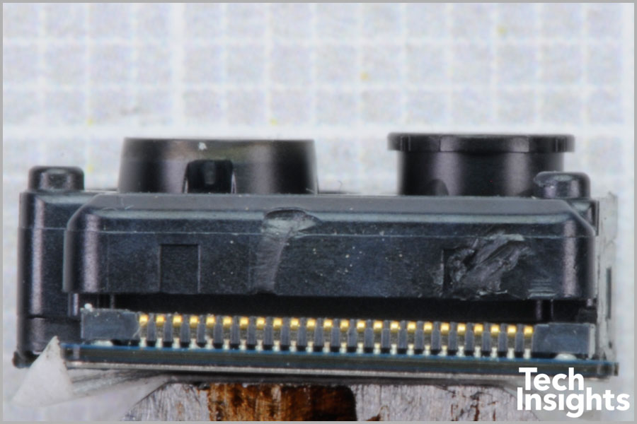
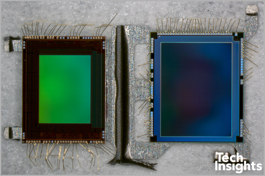
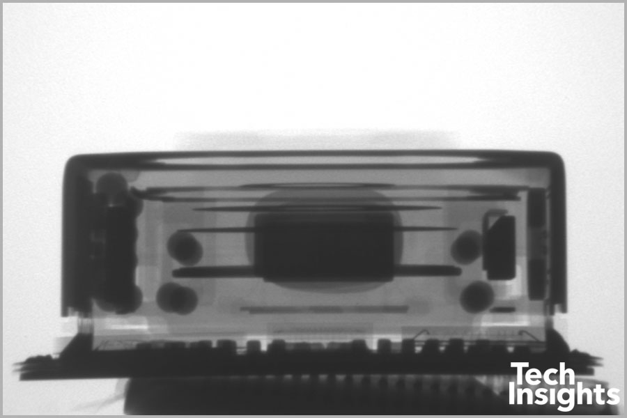
Our lab staff completed preliminary analysis of the 8 MP selfie camera with autofocus and an iris scanner, co-packaged in a 12.5 mm x 11.3 mm x 5.1 mm thick assembly.
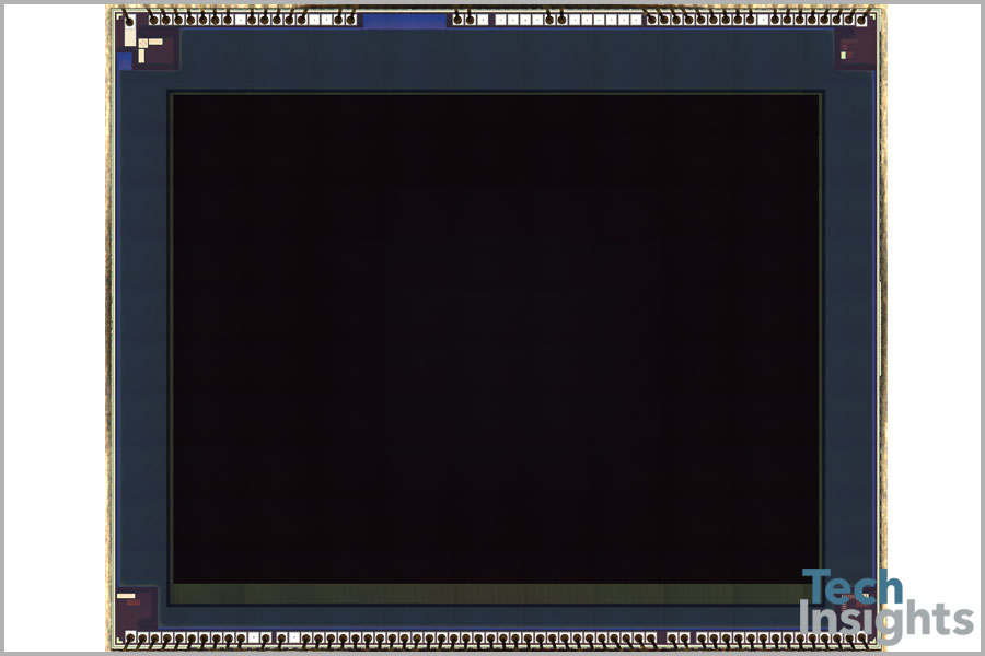
The selfie camera from this G950W model was sourced from Sony. Sony typically does not use conventional die markings on its back-illuminated small-pixel mobile image sensor chips, however the part number has been reported to be the IMX320. The IMX320 is a stacked (Exmor RS) CMOS image sensor (CIS) with a die size of 4.07 mm x 4.82 mm (19.6 mm2) and a pixel pitch of 1.12 µm. Our initial findings suggest it is a conventional back-illuminated (Exmor R) chip, but we’ll be doing more work to learn if it is a stacked (Exmor RS) chip with direct bond interconnect (DBI).
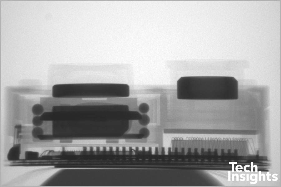
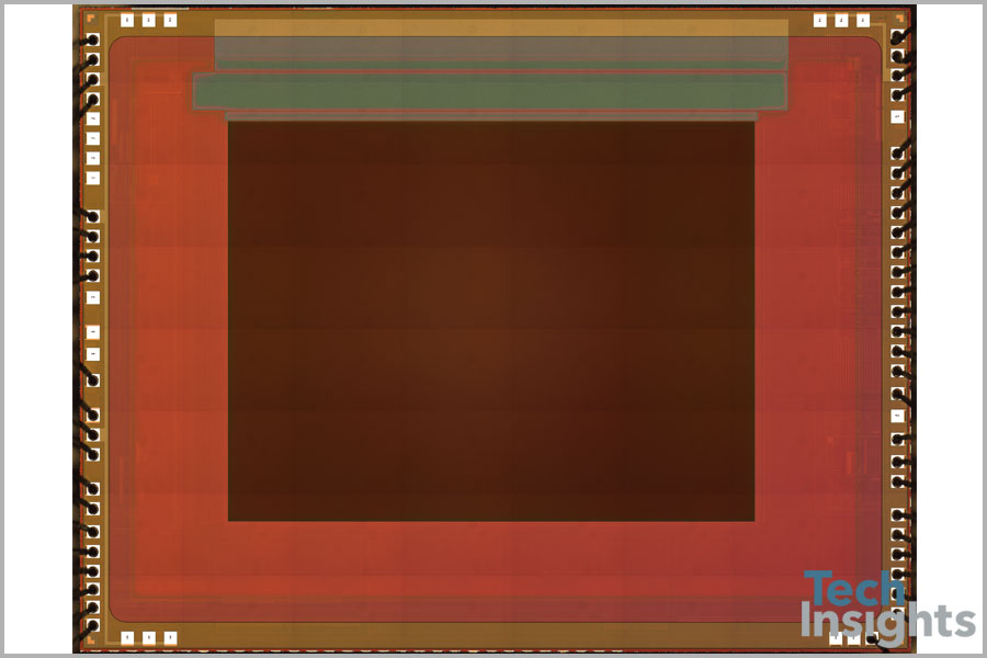
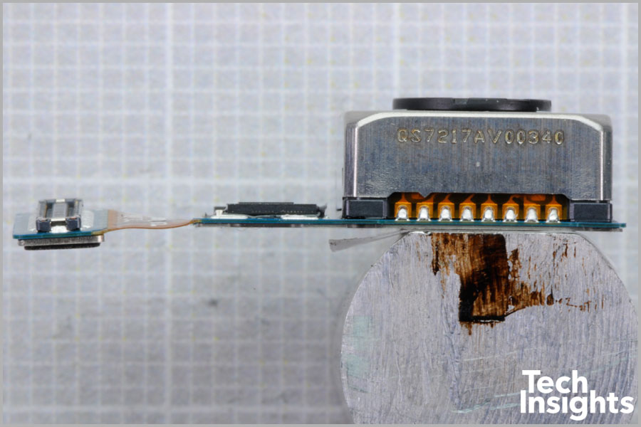
Iris Scanner
The iris scanner chip, while employing new packaging, is the same chip we found in the Galaxy Note 7. The iris scanner die has “S5K5E6YV” die markings, though there is some internal debate as to whether the “V” may in fact be a “U”. Regardless, the die markings are identical to the Note 7’s iris scanner. This chip is a monolithic (non-stacked) back-illuminated CIS featuring a 4.63 mm x 3.55 mm (16.4 mm2) die size and a pixel pitch of 1.12 µm. Additional details are available in our off-the-shelf Device Essentials Image Set and Summary report (DEF-1609-801).
We’ll catch up with an update on the the rear-facing camera as results come in from our labs.
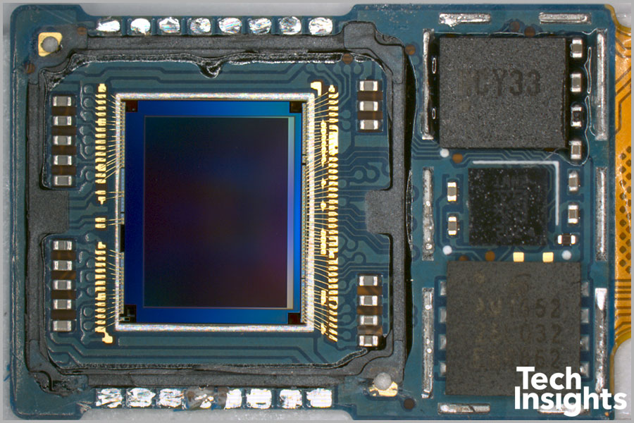
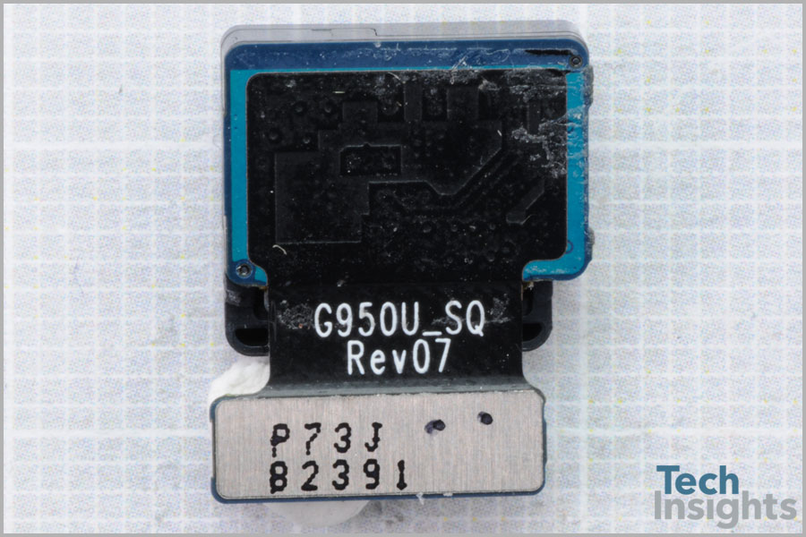
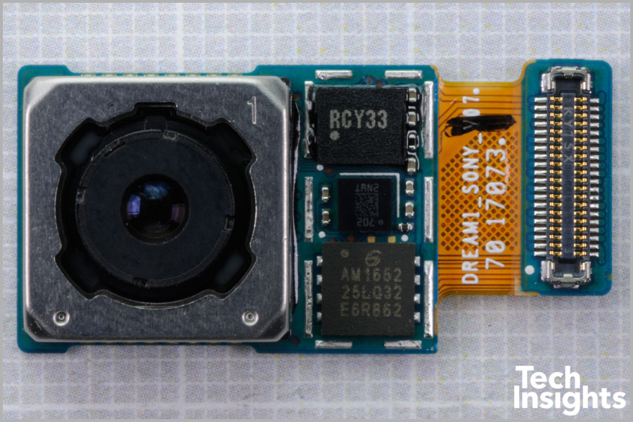
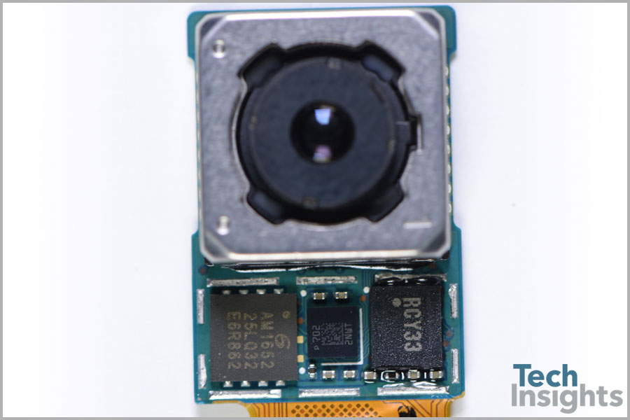
Rear-Facing Camera
Rear-Facing Camera
Neither the Galaxy S8 nor the Galaxy S8+ has a dual rear camera. Now, that makes us happy because it is easier to estimate costs for the main camera, but Samsung is definitely putting a ‘flag’ in the ground with these flagships by not following Apple and Huawei down the dual camera path. The absence of the rear ‘wide’ angle camera shaved around $12.50 from the final bill of materials costs for Samsung.
The SM-G950W rear-facing camera module is 11.3 mm x 11.3 mm x 5.5 mm thick. It contains a stacked, back-illuminated (Exmor RS) Sony die with a die size of 5.64 mm x 6.76 mm (38.1 mm2). While this matches the die size of the Galaxy S7’s Sony IMX260, we do see some minor differences at the die level. As per a SamMobile post, this should be the Sony IMX333. We expect it will be similar to the IMX260, but will be performing more analysis to check for any new customization on this 12 MP, 1.4 MP Dual Pixel CIS.
We also expect to receive more Galaxy S8 phones from other regions soon, which should contain the Samsung S5K2L2 (rear-camera) and S5K3H1 (front-camera) variants. Those details will be published through our Image Sensor subscription service.
Skyworks 2G SKY77365 Power Amplifier Module
Although AT&T announced the shutdown of their 2G cellular network, the appearance of a separate Skyworks 2G RF PAM found in the Galaxy S8 SM-G950W is evidence there is still plenty of interest and need for cell phone OEMs to build devices supporting the legacy network bands. Even if other US cellular carriers follow AT&T and shut off their own 2G networks, 2G cellular will remain active in the UK and many European countries, such as France and Germany, until 2022.
The question is why a separate power amplifier? We asked our in-house RF subject matter expert, Tareq Salim, and his take is this: “...the other multi-mode, multi-band PAMs use amplifiers that are not optimal to work with native 2G GMSK [Gaussian minimum shift keying]. The key success factor for GMSK is having a fixed gain, which the Skyworks SKY77365 achieves.”
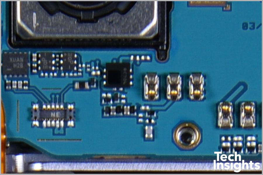
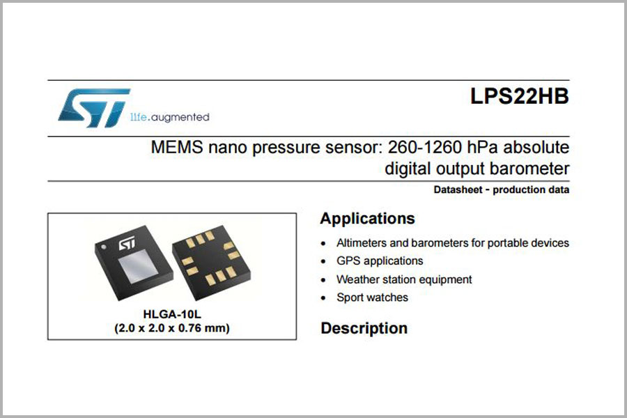
Inertial, Pressure, and Gyroscope Sensors
Inertial, Pressure, and Gyroscope Sensors
So far we have observed a few wins for STMicroelectronics sensors in the S8, beginning with an LPS22HB pressure sensor situated just under the primary image sensor.
We also see an optical image stabilization (OIS) gyroscope with the part number K2G2IS.
The inertial sensor slot also belongs to STMicroelectronics with the LSM6Dl 6-axis inertial sensor, located behind and just under the primary camera, on the opposite side, next to the brand new NXP PN80T NFC controller.
This NFC device is new to us and will be going into the lab as soon as possible. Given that we have analyzed every generation of NXP NFC devices, of course we will be studying this one too, looking for innovation.
NXP PN80T
NFC
We have now decapped the new NXP PN80T NFC IC. Inside, we found two dies in the package: a newly designed PN553 NFC controller and a Secure Element controller (likely SmartMx). According to NXP, the Secure Element is a 40 nm fabbed die. Again, further analysis of these two new NXP dies is to come.
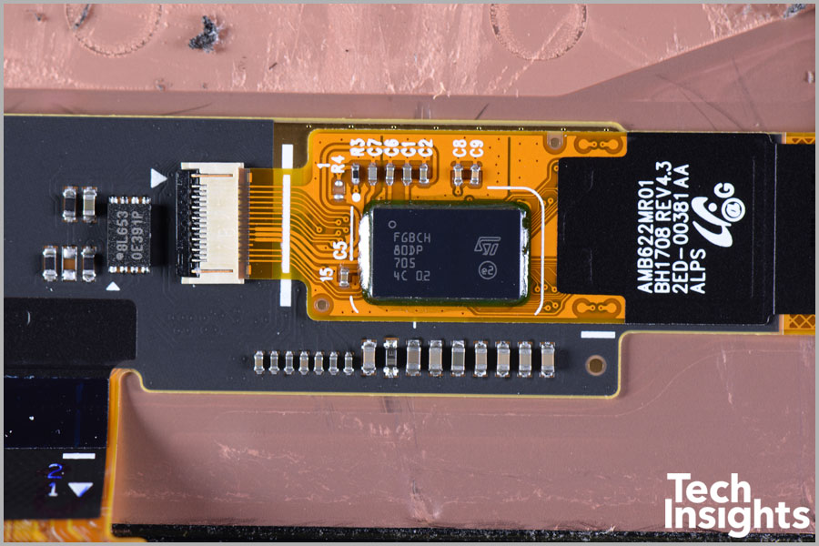
Force Touch and Fingerprint Sensing – Different Solutions
The edge-to-edge, bezel-less viewing space of the Infinity Display means the precious real estate for a physical home key is no longer available. Here, Samsung did follow their two competitors by designing the Galaxy S8 and the Galaxy S8+ with force touch solutions, (3D touch, if you are an Apple fan). On both phones, the force touch is confined to a specific place, right where the physical home keys would have been located.
With both the Galaxy S8 and Galaxy S8+ in our labs, we were able to observe that, while the location was the same, the force touch solutions are different between the two phones. In the Galaxy S8, Samsung uses their own force touch component. The Galaxy S8+, however, employs an STMicroelectronics fingerprint and force touch sensing chip from the Finger Tip product family.
If there were any cost savings gained by not using a separate home key/fingerprint sensor assembly, the larger panel and more pixels of the Infinity Display have still resulted in higher costs. The Galaxy S8 costs are around 40% and 20% higher than the Galaxy S7 and Galaxy Note 7, respectively.
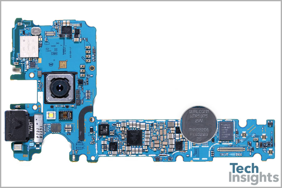
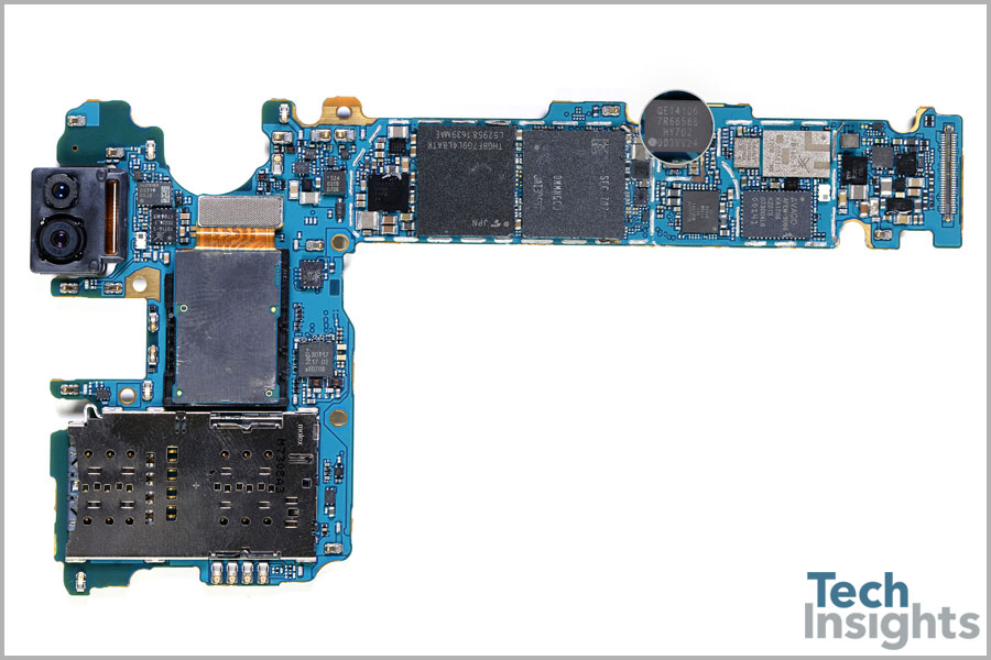
Board Shots and Parts
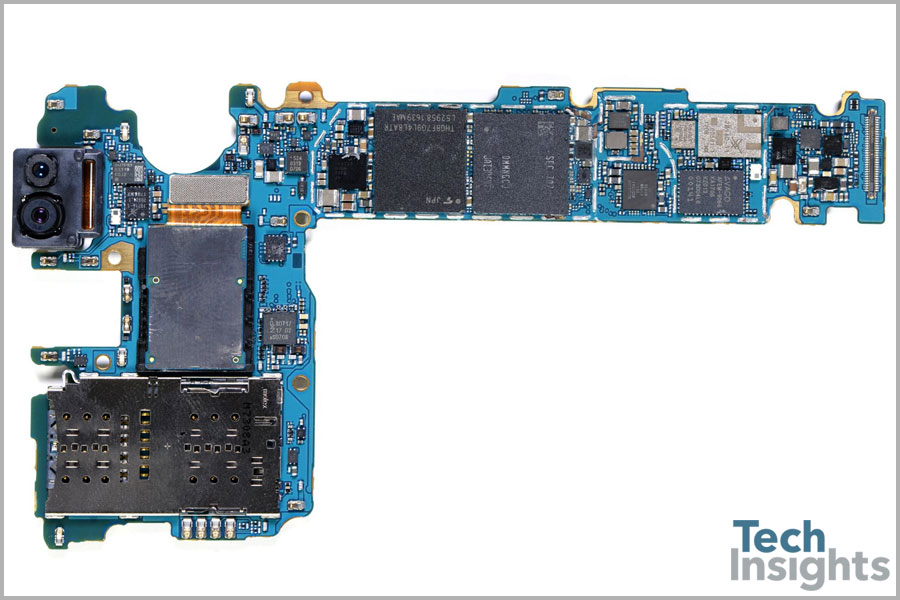
Samsung Galaxy S8 Board
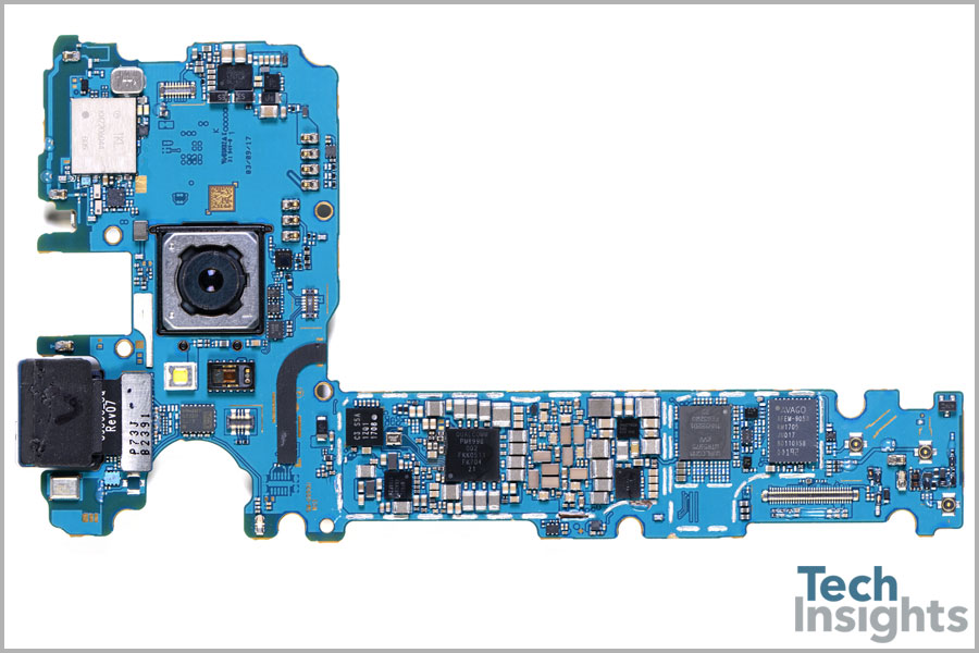
Here is a look at what we have uncovered thus far. Above are images of the front and back of the printed circuit board (PCB), from which we identify the following parts:
| Manufacturer | Part Number | Function |
|---|---|---|
| Qualcomm | MSM8998 | Application processor |
| Samsung | K3UH5H50MM-NGCJ | 4 GB LPDDR4X |
| Samsung | S6SY761X | Touch screen controller |
| Samsung | S5C73C3 | Image processor |
| Qualcomm | WTR5975 | RF transceiver |
| Qualcomm | PM8998 | PMIC |
| Qualcomm | PM8005 | PMIC |
| Maxim | MAX77838 | PMIC |
| Samsung | S2MPB02 | PMIC |
| Broadcom | AFEM-9053 | Power amplifier |
| Broadcom | AFEM-9066 | Power amplifier |
| Skyworks | SKY78160-11 | Power amplifier |
| Skyworks | SKY77365 | 2G power amplifier |
| Toshiba | THGBF7G9L4LBATR | 64 GB universal Flash storage |
| Qualcomm | QET4100 | Envelope tracking power supply |
| Qualcomm | WCD9341 | Audio codec |
| Maxim | MAX98506BEWV | Audio amplifier |
| NXP | PN80T | NFC controller |
| STMicroelectronics | LPS22HB | Barometer |
| STMicroelectronics | K2G2IS | OIS gyroscope |
| STMicroelectronics | LSM6DL | 6-axis inertial sensor |
| STMicroelectronics | FGBCH80DP | Finger Tip touch screen controller |
| Knowles | SPH0644LM4H-1 | Microphone |