Posted: May 18, 2017
Contributing Authors: Jeongdong Choe, Senior Technical Fellow
Figure 1: Xpoint Memory Package
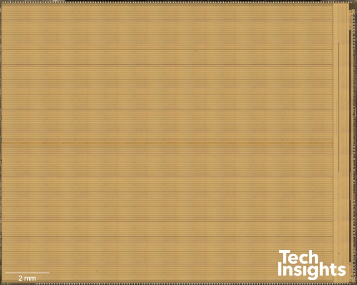
Figure 2: Xpoint Memory Die (16 GB)
TechInsights recently acquired and tore down an Intel OptaneTM M.2 80mm 16GB PCIe 3.0 and discovered a 3D X-Point memory die in the package. This is the first commercial 3D Xpoint product from Intel and Micron. The Intel 3D X-Point memory package size is 241.12 mm2 (17.6 mm x 13.7 mm) and a single X-Point Memory die is contained within. The 3D X-Point Memory die measures 206.5 mm2 with a 16.16 mm length and a 12.78 mm width. Memory efficiency in the die is 91.4% which is higher than the Samsung 3D 48L V-NAND (70.0%) and the Intel/Micron 3D FG NAND (84.9%). Memory density of the 3D Xpoint Memory is 0.62 Gb/mm2 which is lower than commercial 2D and 3D NAND products (2.5 Gb/mm2 for Toshiba/SanDisk and Samsung 3D 48L TLC NAND, and 1.28 Gb/mm2 for Toshiba/SanDisk 2D 15nm TLC NAND). However, compared to DRAM products, the 3D Xpoint memory density is 4.5 times higher than DRAM products with the same 20 nm technology or 3.3 times higher than Samsung’s 1x nm DDR4. Xpoint Memory products use 20 nm technology node for both WL and BL with 0.00176 µm2 cell size which is about half of the DRAM cell size. This is due to a stackable memory cell and 4F2 instead of 6F2 being used for memory cell array design.
Product Information: Intel 3D XPoint Analysis Report
This product brief summarizes the deliverables that we intend to build as well as some additional commentary on the technological relevance of the part.
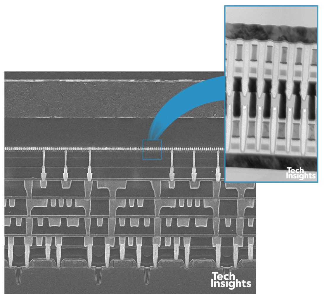
Figure 3: X-point Memory Array X-section SEM and TEM images
Intel Xpoint Memory is a PCM (Phase Change Memory) with a double storage-selector stacked memory cell between metal 4 and metal 5. GST-based materials are used for the storage, while As (arsenic) doped chalcogenide materials (Se-Ge-Si) are used for the selector in which As might be used to suppress crystallization. This is likely a type of Ovonic Threshold Switch (OTS) structure. We found that the 3D Xpoint memory layers are placed between metal 4 and metal 5 and connected with a few selector contact plugs on metal 4. We’ll be digging deeper into the device to find more innovative technology, and we’ll share that with you in the near future.


