Posted: April 2, 2015
Contributing Authors: Dick James and Daniel Yang
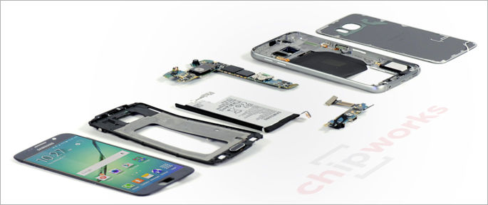
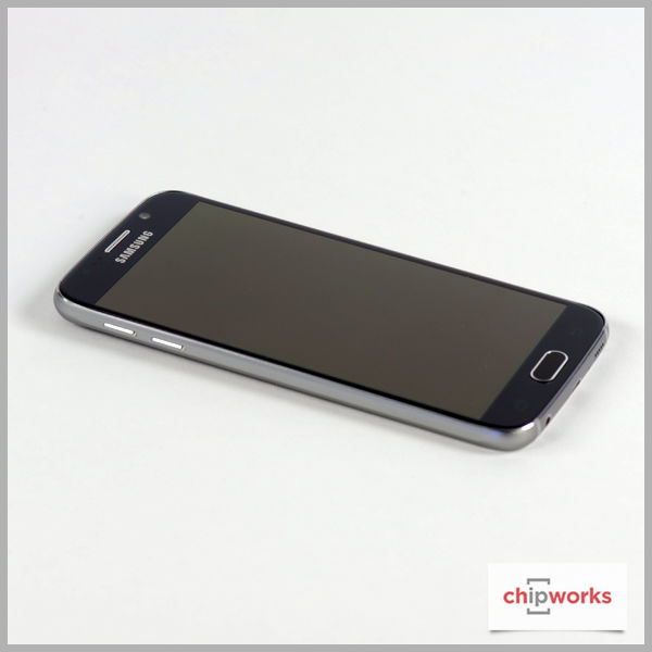
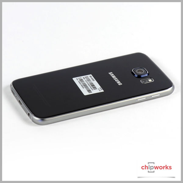
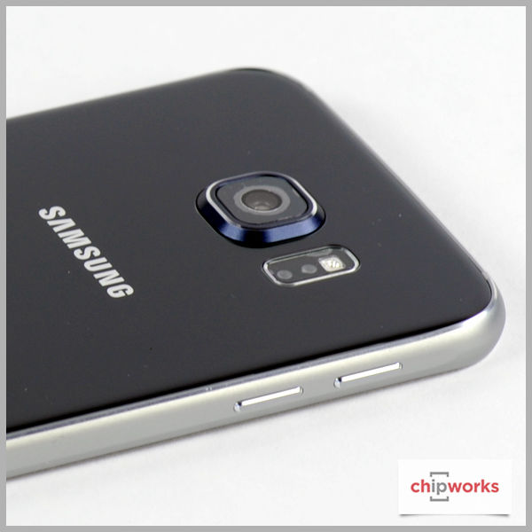
Samsung Galaxy S6 Teardown
The much anticipated Samsung Galaxy S6 has made an early appearance in our teardown labs this morning – thanks to the diligent skills of our trusted logistics guru. We got our hands on the 4G+ version, the SM-G920I, with what Samsung claims is the world’s first octa-core 64 bit operating system. There is a wide array of industry buzz surrounding this flagship smartphone and our focal point for this teardown will be on the Exynos 7420 application processor. We will also be featuring semiconductor design wins of other devices that we’ve identified. Stay tuned for updates as more analysis comes out of our labs!
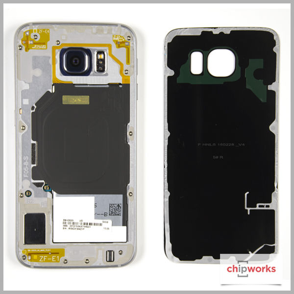
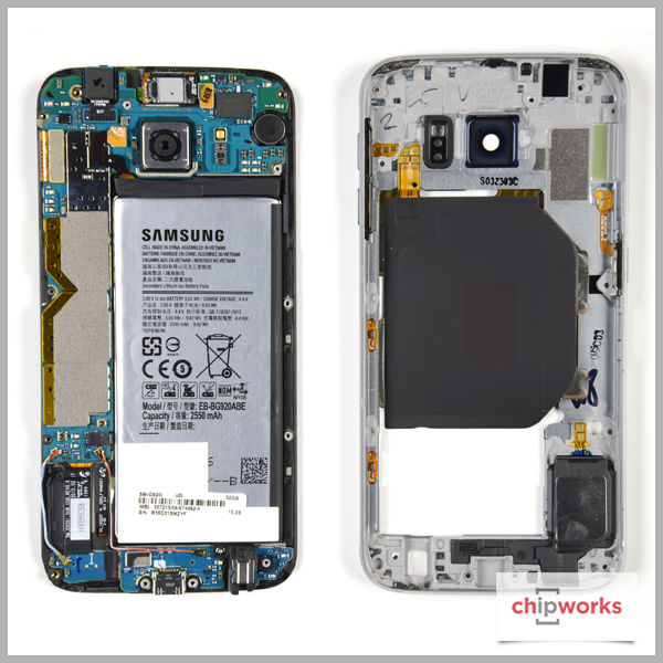
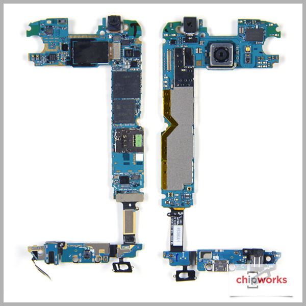
Design Wins
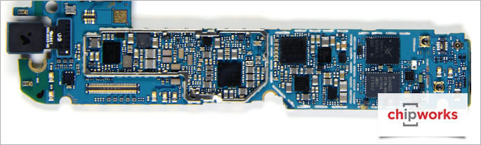
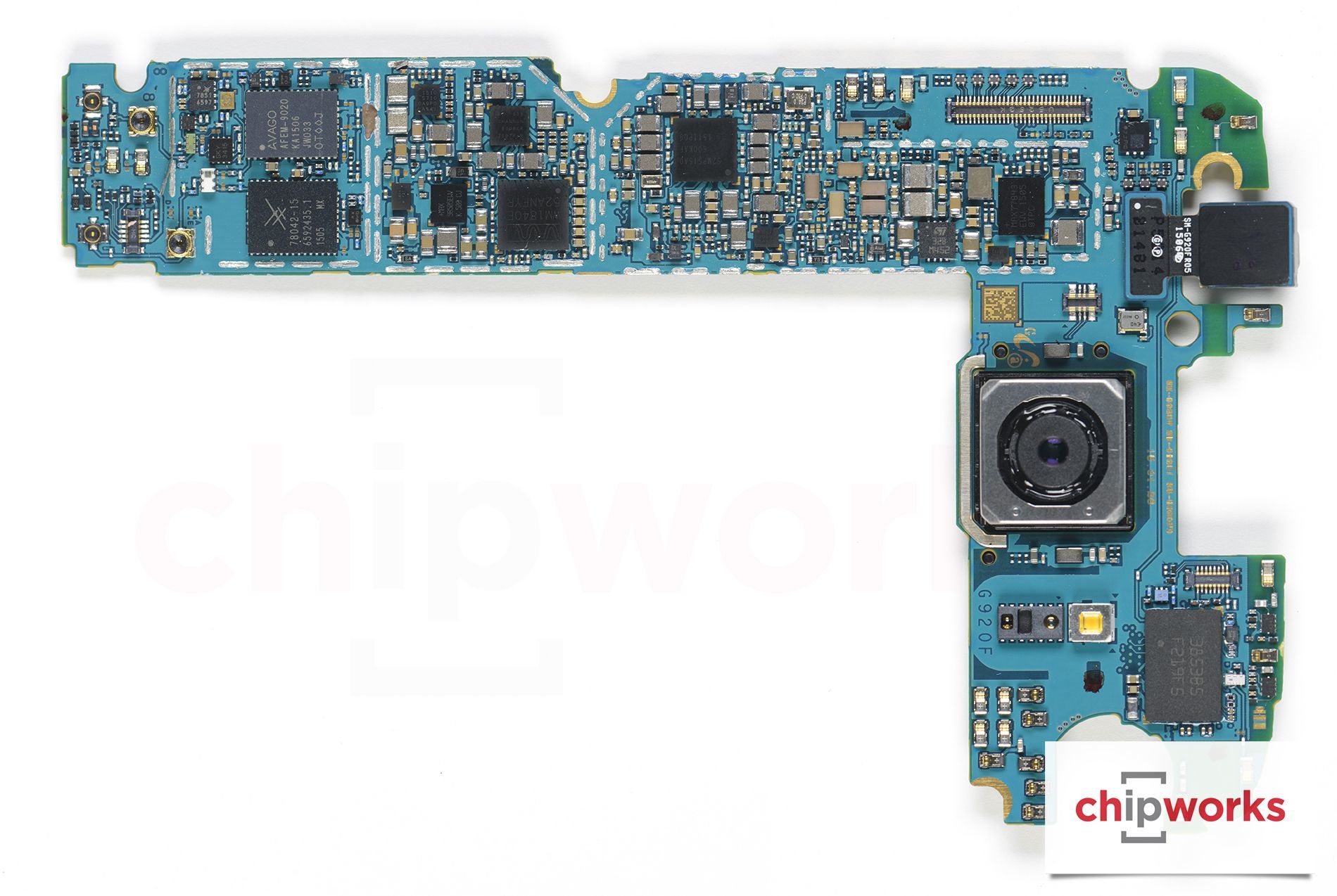
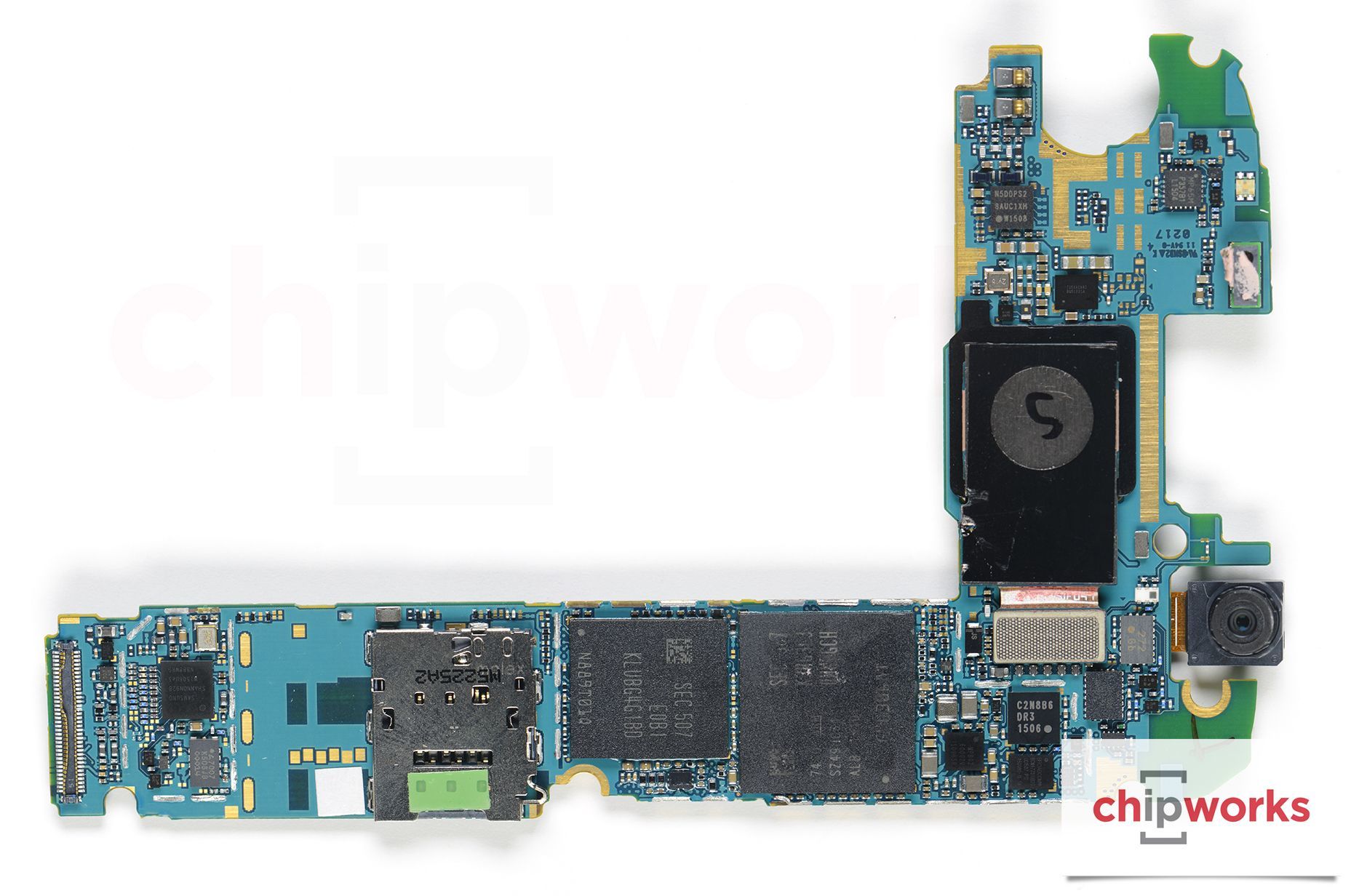
We’ve been able to identify multiple chips inside the Galaxy S6:
- Samsung Exynos 7420 SoC
- Samsung K3RG3G30MM-DGCH 3Gb LPDDR4 SDRAM and Samsung KLUBG4G1BD 32GB NAND Flash
- Samsung Shannon 333 Modem, Shannon 533 PMIC, Samsung S2MPS15 PMIC, Samsung Shannon 928 RF Transceiver and Samsung Shannon 710 Envelope Tracking IC
- Broadcom BCM4773 GNSS Location Hub
- InvenSense MPU-6500 Gyro + Accelerometer
- Skyworks SKY78042 Multimode Multiband (MMMB) Front-End Module (FEM)
- Avago AFEM-9020 PAM and Avago ACPM-7007 PAM
- Samsung C2N8B6 Image Processor
- Maxim MAX98505 Class DG Audio Amplifier and Maxim MAX77843 Companion PMIC
- Samsung Electro-Mechanics 3853B5 Wi-Fi Module
- N5DDPS2 (Likely Samsung NFC Controller (P/N needs to be confirmed)
- Wolfson WM1840 Audio CODEC
- Texas Instruments BQ51221 Single Chip Wireless Power Receiver
- Skyworks SKY13415 Antenna Switch
- STMicro FT6BH Touch Screen Controller
Samsung is continuing the trend of introducing their own silicon into their phones. Now we not only have the APU and memory, but also the modem, two PMICs (power management ICs), an RF transceiver chip, an envelope tracking IC, likely the NFC controller, and an image processor (and a Samsung Electro-Mechanics Wi-Fi module).
We see the Galaxy S6 using an STMicroelectronics Touch Screen Controller. This is not a complete surprise to us as we had seen earlier Samsung making use of STMicroelectronics touch screen solution inside the Galaxy Note Neo 3 models in the middle of last year. Clearly the STMicroelectronics solution was a good one for Samsung as they have chosen it again for the Galaxy S6. Congratulations STMicroelectronics!
Design Wins
Samsung Exynos 7420 Application Processor
Samsung Exynos 7420 Application Processor
The Samsung Exynos 7420 application processor is reportedly fabbed in Samsung’s 14 nm FinFET process. It is in the lab and as soon as we get a good cross-section showing finFETs we will be posting it! This is what Samsung has shown so far.
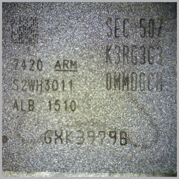
Which is not exactly specific! In the meantime here’s the package marking of the package-on-package.
The layout of this is quite unusual – normally the memory marking (SEC 507 etc.) is in lines of text above the APU marking (7420 etc.), not in a diagonally opposed block.
Samsung Exynos 7420 Application Processor
Which leads me into the speculation that maybe the 7420 is out of GLOBALFOUNDRIES, rather than a Samsung fab in Korea or Texas. Could ALB be short for Albany (NY)? Is the G in the lot code short for GLOBALFOUNDRIES? That all seems rather unlikely, but if Samsung wants to switch on the volume quickly in anticipation of huge volumes for the S6, what better way than to use three fabs? They did sound very confident in their last quarterly analyst call, saying that they expect 14-nm to be 30% of the LSI line capacity by year end. And there are lots of rumours about Qualcomm using the Samsung 14-nm process.
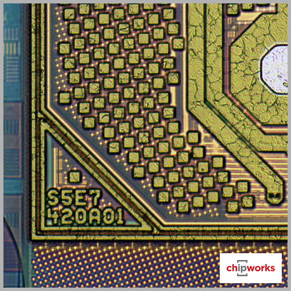
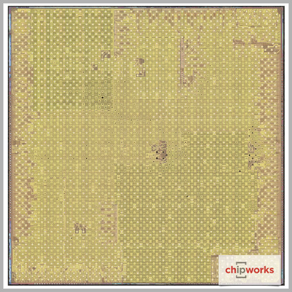
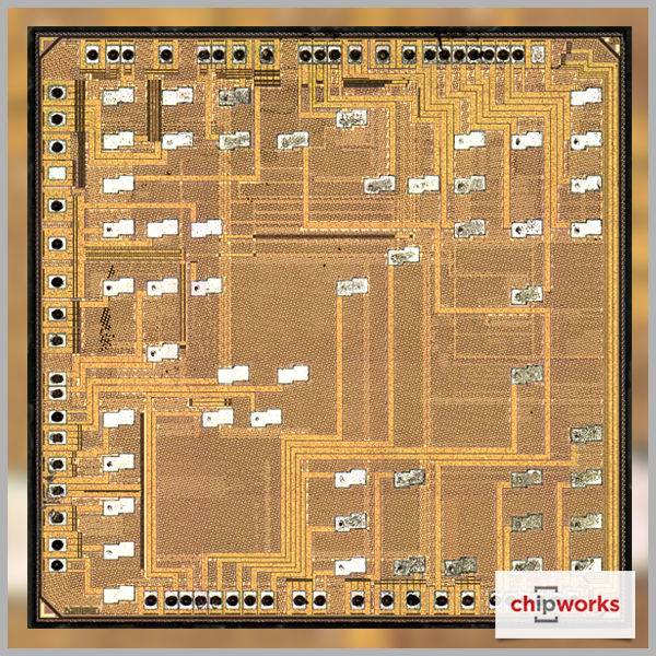
Now we have a die photograph and the die mark.
The functional die size is ~78 mm^2, which compares well with the 118.3 mm^2 of the Snapdragon chip used in the Galaxy S5, and the 113 mm^2 size of the 20-nm Exynos 5433. If the 7420 was a straight shrink of the 5433, we’d expect it to be 55 – 60 mm^2, but the back-end metallization stack is reported to be similar to the 20-nm planar process, so a full 50% shrink is unlikely (and the analog regions never shrink as well as digital anyway). We’ll have to wait until we see the floorplan to see how much functionality the two parts have in common.
FinFET
FinFETS or not FinFETS?
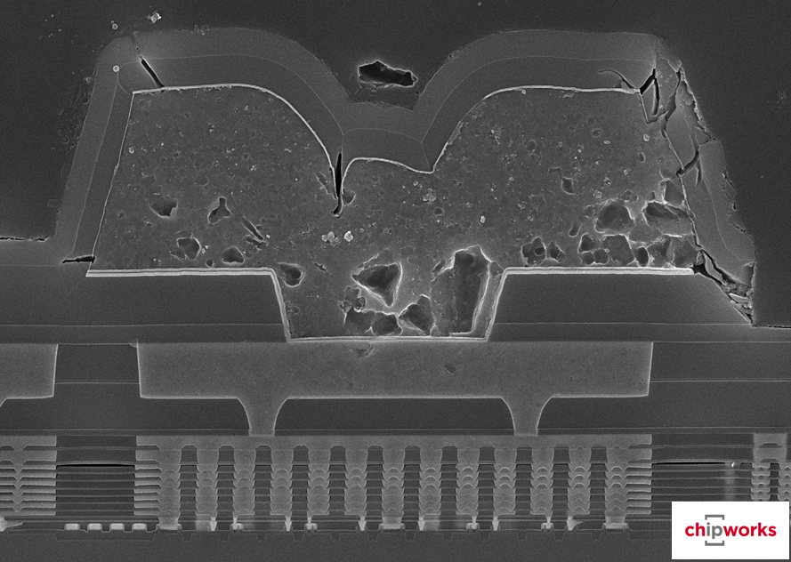
Our guys in the lab made their usual exceptional effort in enabling us to see what the process looks like – within a few hours of getting the phone in-house, we have a decapsulated part and a cross-sectional sample under the microscope.
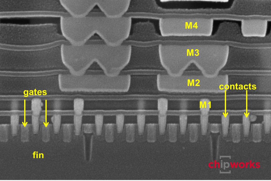
The Exynos 7420 uses 11 layers of metal, as you can see from the die seal cross-section above. Now let’s look at the transistors.
And we do have finFETS! This section is parallel to the fins, and across the gates. The bottoms of the contacts approximately indicate the top edge of the fin, and we are seeing the gates wrapped over and further down the sidewalls of the fin than the contacts appear to go. We will need another section orthogonal to this one to see if we have the type of epi growth in the source-drains that Intel uses.
This makes Samsung the second in line to get finFETs into volume production; they have successfully taken their 20-nm, first-generation, gate-last, high-k, metal-gate stack and adapted it to a first-generation fin structure. We will need more detailed images to see whether the fins have vertical or sloped sidewalls, and how close to the Intel model they are, but those will come in the fullness of time when we have completed our full analysis and published our report.
Cameras
Cameras
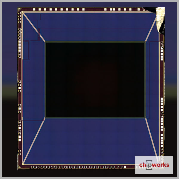
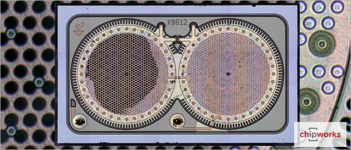
As reported by phonearena.com, the Galaxy S6 uses a Sony IMX240 rear camera while the front-facing camera is a Samsung S5K4E6. The IMX240 is a 16 MP stacked chip, back-illuminated CMOS image sensor with a die size of 7.09 mm x 4.68 mm (33.2 mm2). The Exmor RS sensor features 1.12 µm pitch pixels and an on-chip phase detection pixel array for fast autofocus.
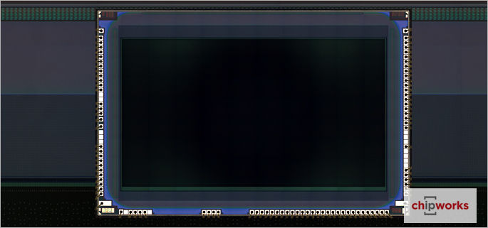
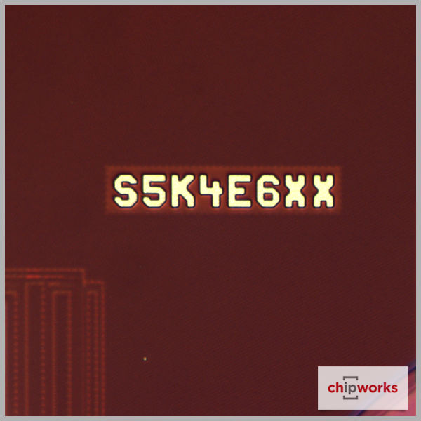
The Samsung S5K4E6 is a 5 MP back-illuminated CMOS image sensor with a die size of 5.31 mm x 5.87 mm (31.2 mm2). The pixels have a 1.34 µm pitch.
NFC Controller
NFC Controller
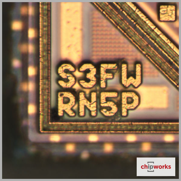
In last week’s initial teardown blog, we said that the NFC Controller was likely a Samsung device. We can now confirm that it is in fact the Samsung NFC Controller S3FWRN5P. According to Samsung, the S3FWRN5P is the company’s “fourth-generation NFC solution features significantly improved RF performance, showing an increase of about 100 percent over its predecessor in card mode and 20 percent in reader mode, respectively”. S3FWRN5P. Chipworks has produced a few NFC Controller reports, including NXP PN544/547/548, Broadcom BCM2079x, and Samsung S3FWRN5. Meanwhile, Chipworks also has all the world’s mass-produced NFC Controller devices torn down from consumer electronics products (including MediaTek MT6605 and STMicro ST21NFCAH etc.) although we have not produced reports yet.
We also confirmed that Knowles won two microphone sockets in the Galaxy S6 SM-G920I.
Aleady a subscriber?
TechInsights Teardown subscribers already have access to exclusive content in the TechInsights Platform.
Interested in a subscription?
TechInsights offers subscriptions to the broadest range of analysis and expert commentary. Contact us to learn about our many subscription offerings.