Posted: November 22, 2013
Xbox One
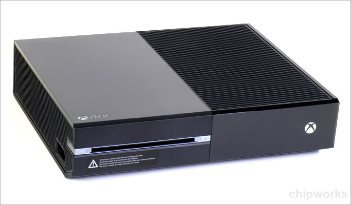
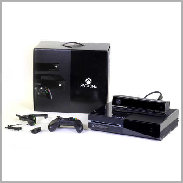
It's clear we're in the run-up to the gift-giving season, with multiple launches of tablets and gaming systems. Last week was the turn of the Microsoft Xbox One, and it's hard to believe it's been twelve years since the first Xbox was launched, and eight years since the Xbox 360. There have been a few upgrades since the first 360, but now it's time for a complete rework.
Style is a personal thing, but the new console looks cleaner and simpler than the earlier generations, although it still has a separate power brick to get in the way, unlike the Sony PS4.
Inside
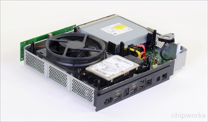
What's Inside?
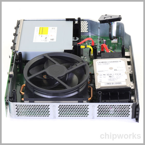
Inside we can see the Philips & Lite-on Blu-ray/DVD drive and a Samsung 500 GB hard disc drive, and of course the cooling fan, with parts of the heat pipes visible. At the top left in the first thumbnail image is the WiFi board, linked by a slim coax wire to an antenna board at the front right.
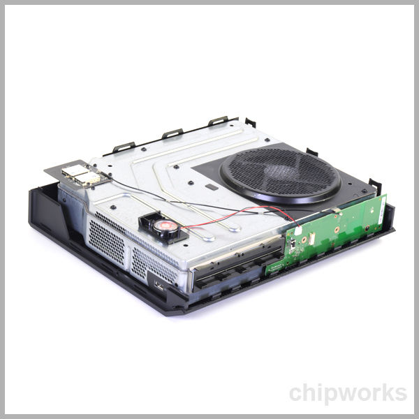
Main Board
The Main Board
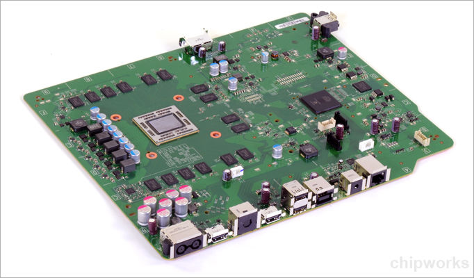
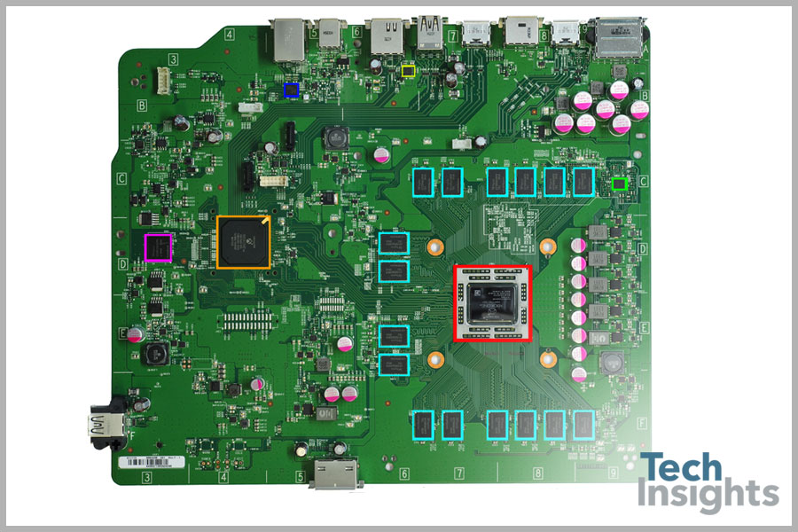
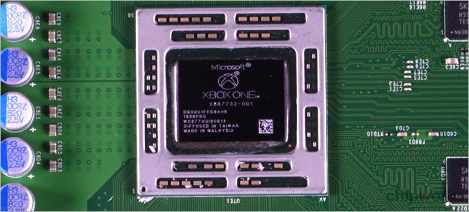
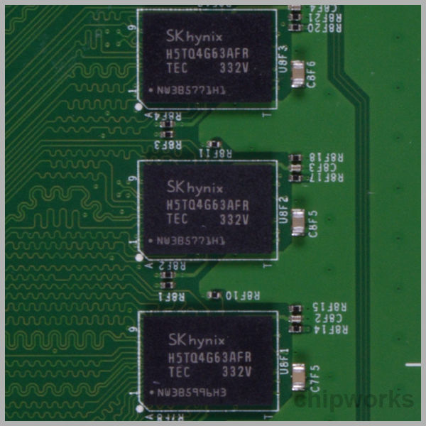
Now we get the heatsink off and the motherboard out, and as expected the C/GPU processor is surrounded by DRAM chips, in this case 16 SK Hynix 4-Gb DDR3 SDRAMs, giving a total of 8 GB dynamic memory. The other large die on the board is the Southbridge chip that acts as the interface with most of the peripherals, including the Kinect.
Looking at the WiFi board, Marvell has got the design wins with a pair of Avastar chips, a 88W8897M WLAN/BT/NFC SoC and 88W8782U WLAN SoC. A close look at the board shows antennas built in, confirming the MIMO, but we haven't heard anything about the device having Bluetooth or NFC capability. Presumably a case of buying a part that's available, rather than customising (or maybe games will become tap & go in the near future..).
- Xbox X887732-001 Processor DG3001FEG84HR (includes AMD "Jaguar" Cores and AMD Radeon Graphics GPU)
- SK Hynix H5TQ4G63AFR 4 Gb (512 MB) DDR3 SDRAM (total of 16 x 512 MB = 8 GB)
- Xbox X861949-005 T6WD5XBG-0003 Support Processor
- SK Hynix H26M42003GMR 8 GB e-NAND Flash
- ON Semiconductor NCP4204 GAE1328G Integrated Power Control IC
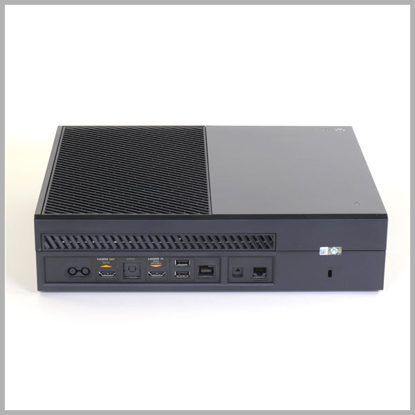
- Realtek RTL 8151GNM Ethernet Controller
- Texas Instruments TPS2590 - 3-V to 20-V High-Current Load Switch for Hotswap Management
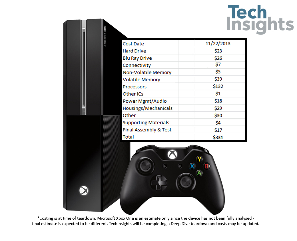
Microsoft Xbox One - Quick Cost Estimate (BOM)
Main Processor
The Main Processor
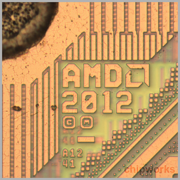
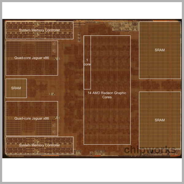
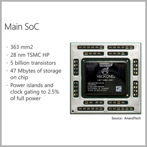
Zooming in on the main board, we can identify the DRAM as SK Hynix H5TQ4G63AFR DDR3 SDRAM. The main processor chip has the same style of heat-dissipating package as the PS4 CPU, and the die is actually larger at 363 sq. mm. (vs 348 sq.mm. for the PS4 die), but with 47 MB of SRAM in there that's not surprising.
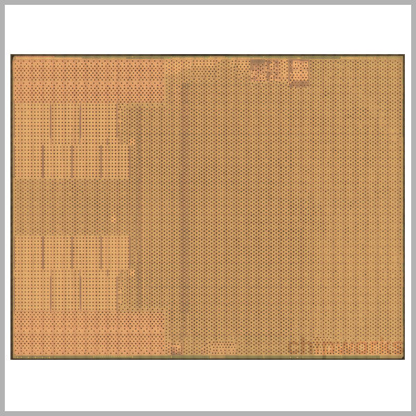
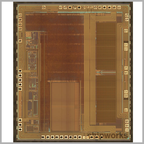
Much has been made of the different memory architectures between the Xbox One and Playstation 4. Indeed, according to technology sites such as Anandtech and Red Gaming Tech, the higher complexity of the Xbox memory architecture is the likely culprit behind the lower resolutions of some of the Xbox launch titles, compared to the same games running on a PS4. Call of Duty Ghosts, for example, is said to run at 1080p on the PS4, but only at 720p on Microsoft’s console.
Sony’s PS4 uses a unified 8GB main system memory accessed in parallel by the either the CPU or GPU, which sit together on one die, through a relatively high-speed GDDR5 memory interface. The Xbox, although it also uses an 8GB main system memory to which both the CPU and GPU have access, chose a lower-power but lower performance DDR3 interface. To compensate for this slower main memory, a 32MB ultra high speed dedicated graphics memory is included on die as an embedded SRAM block, together with the CPU and GPU. Necessarily, programming for such an architecture will be more complex. However, the theoretical peak performance of the two systems could be very similar. Others can more usefully comment on ultimate performance, while Chipworks has the privilege of being about to share the die images of these monster processors with you. The images below include an annotated view of the poly layer of the Xbox C/GPU/SRAM die. See our PS4 teardown for the corresponding image of Sony’s C/GPU.
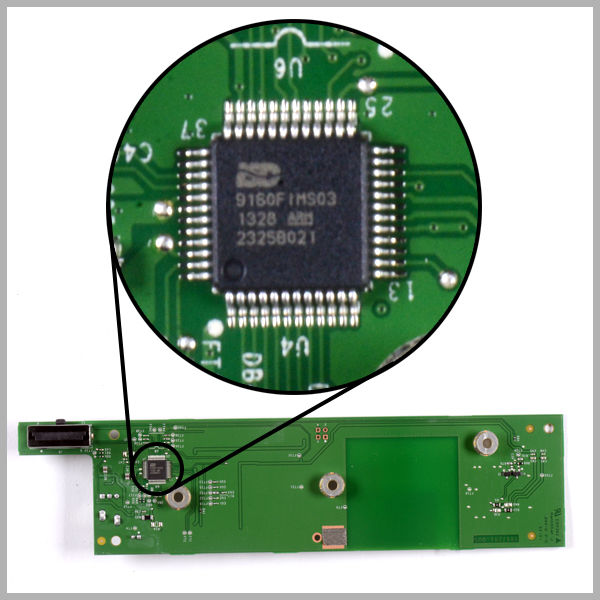
The last two images in the row are from the back side of the antenna board noted earlier; there's only one IC on there, but after a bit of digging it appears that it's the audio user interface chip, an ISD9160 from Nuvoton. That accords with the enhanced voice commands claimed for the Xbox One.
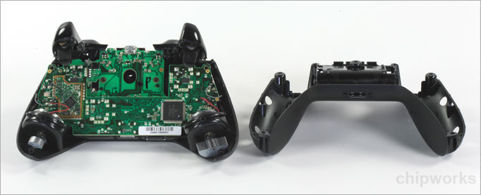
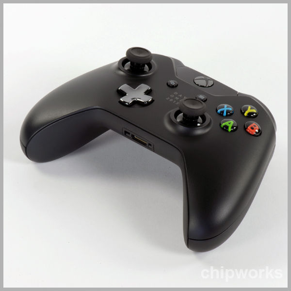
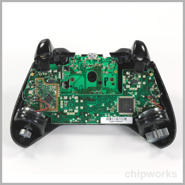
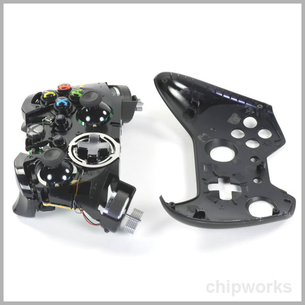
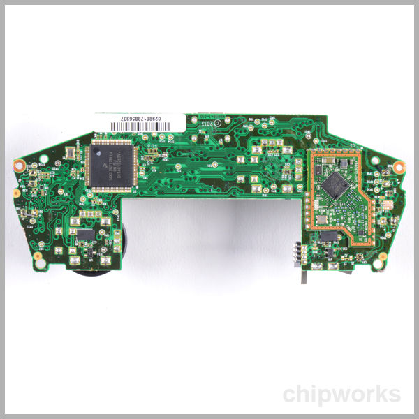
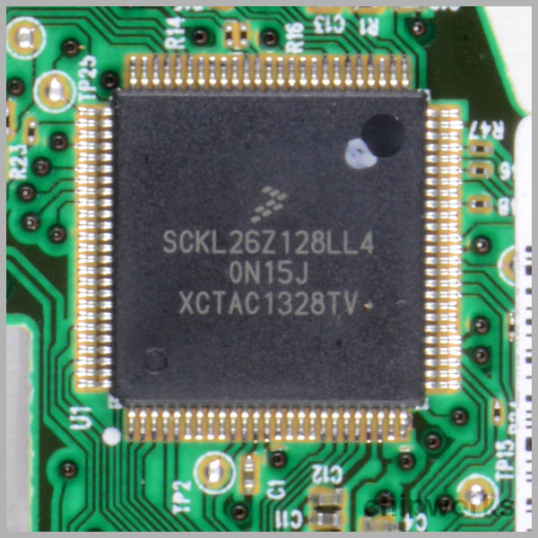
The Controller
The Controller
The controller, as usual, has a low chip count; a Freescale SCKL26Z128LL4 Kinetis ultra-low power microcontroller, with a 32-bit ARM Cortex M0+ core and 128 KB embedded flash, and a custom Microsoft X872519 WiFi chip on a separate sub-board.
The Kinect 2.0 camera system is quite a complex bit of gear, and justifies a separate teardown account of itself, so we'll get into that next.