Posted: March 1, 2018 - Updated: March 21, 2018
Contributing Author: Daniel Yang & Stacy Wegner
Samsung Galaxy S9
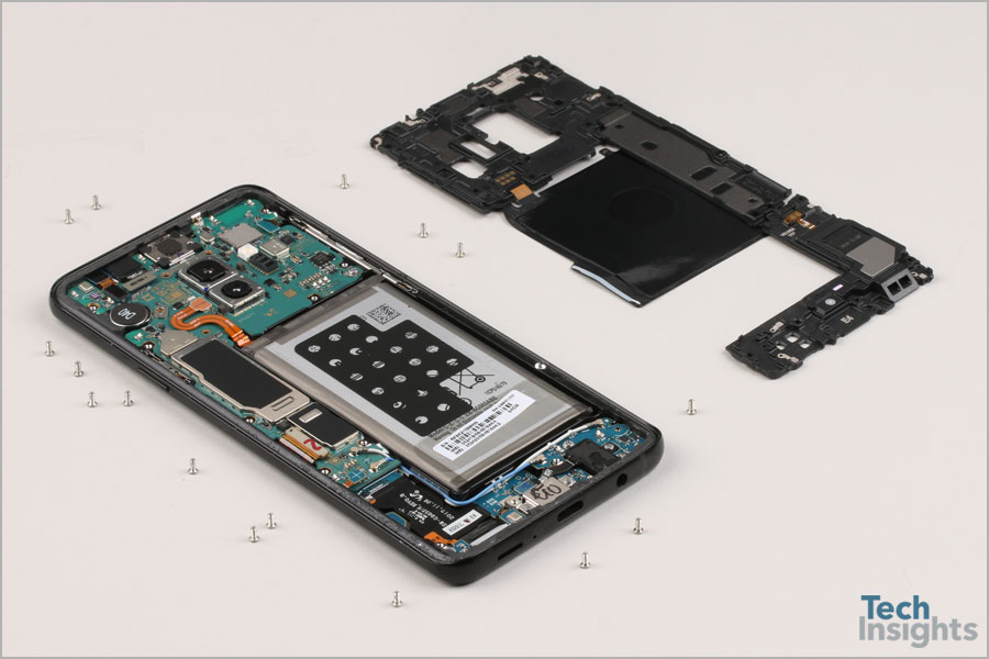
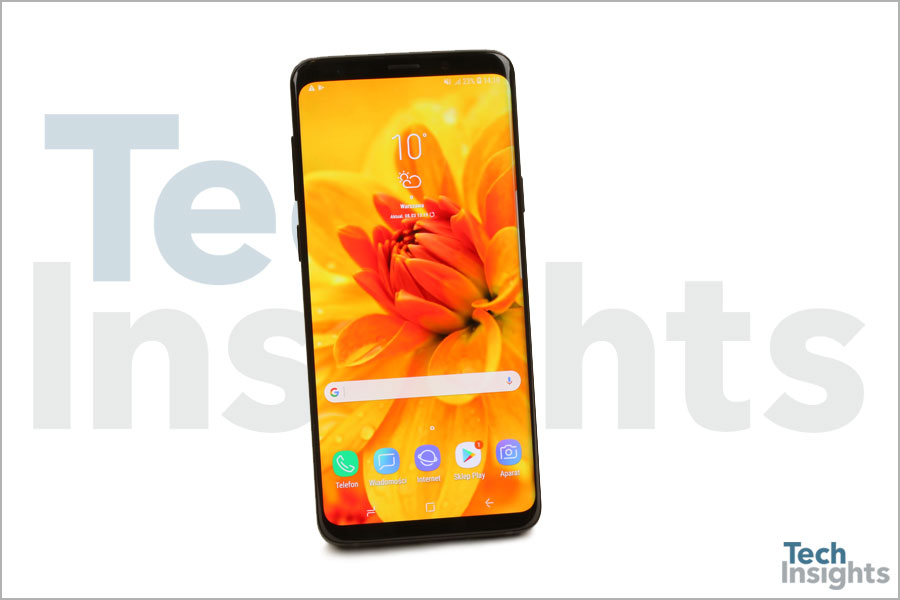
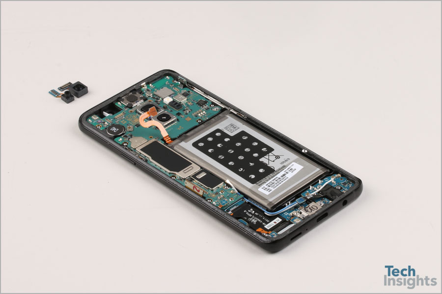
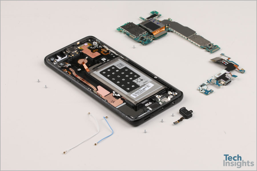
As we reported in our MWC18 blog, Samsung’s flagship Galaxy S9 and S9+ smartphones were officially unveiled in Barcelona on Feb 25, 2018 at the Mobile World Congress (MWC) 2018 pre-event. Our procurement team managed to get one Galaxy S9+ (Model: SM-G965F/DS, 64GB) in our hands early for a quick teardown. Our teardown experts did an amazing job in separating the phones into pieces so quickly, so we have the chance to share with you our early findings of what’s inside the Samsung flagship Galaxy S9+.
We will continue to update this blog as we identify additional parts in the phone. Check back regularly for updates.
Application Processor
We tore down multiple versions of the Galaxy S9+. Samsung has continued with their dual-sourcing strategy, including the Exynos AP in European models, and Qualcomm’s Snapdragon in US models. The table below compares the major components of the two models:
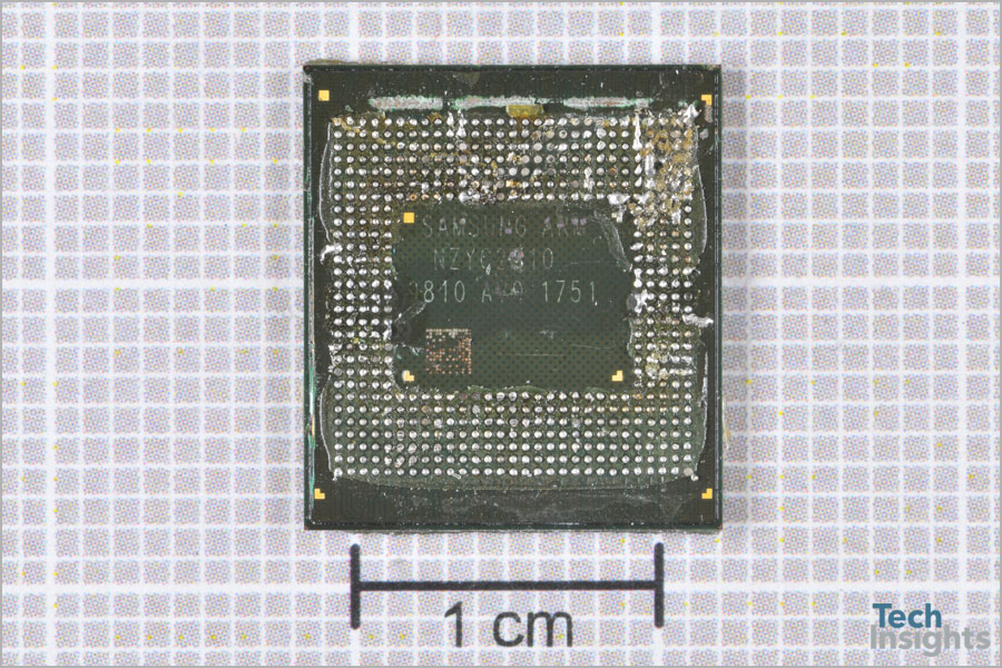
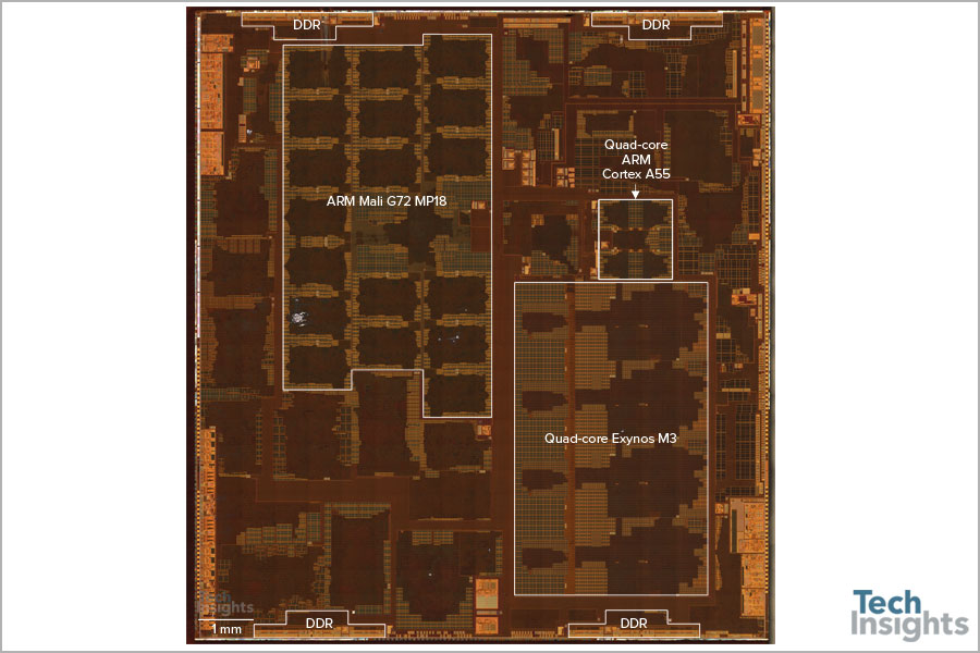
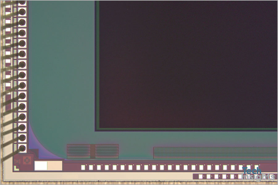
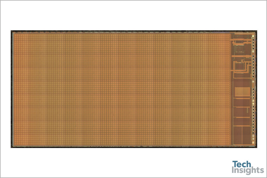
Samsung’s application processor Exynos 9810 inside the Galaxy S9+
Exynos 9810
Our Galaxy S9+ model includes Samsung's own Application Processor Exynos 9810. The Application Processor module is a Package-on-Package (PoP) with Samsung's own 6GB LPDDR4X SDRAM K3UH6H60AM-AGCJ. We were hoping to see the rumored DDR5, but this version of the phone still includes the LPDDR4X.
The Exynos 9810 is fabbed in Samsung's 2nd generation 10nm FinFET process 10nm LPP. According to Samsung, the 10LPP process technology allows up to 10% higher performance or 15% lower power consumption compared to its first generation 10nm LPE (Low Power Early).
TechInsights has already analyzed the Samsung 10LPE process technology found inside the Qualcomm Snapdragon 835 and Samsung Exynos 8895 APs. We have published a few competitive technical analysis reports such as Digital Functional Analysis Report (DFAR), Advanced CMOS Essentials (ACE), and Transistor Characterization Report. We will also analyze the Samsung 10LPP process in a few report formats.
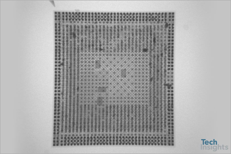
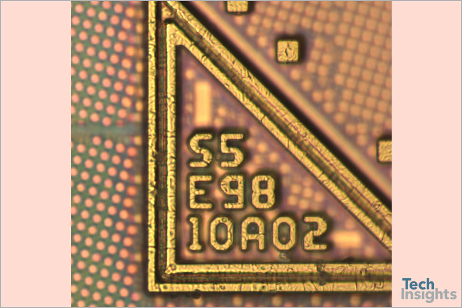
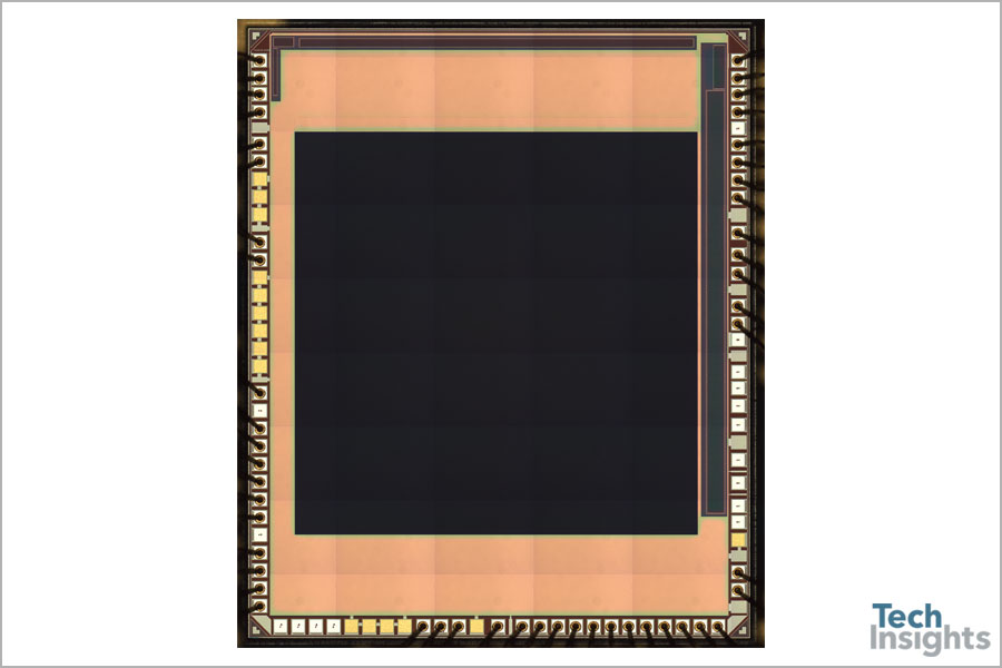
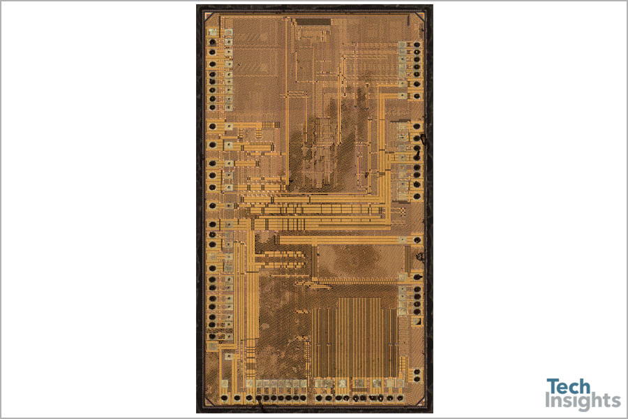
We have decapped the Samsung Exynos 9810 AP PoP and gotten the images of the AP/Modem die with a die mark S5E9810A02. The die size (seal) is 10.37 mm x 11.47 mm = 118.94 mm2, a slight bigger than the previous Exynos 8895 AP/Modem die S5E8895A01’s seal die size 10.50 mm x 9.87 mm = 103.64 mm2.
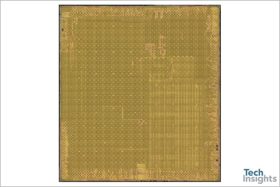
The overall die size (from die seals) increased by 15%. This is expected because the 10LPP technology is a performance boost compared to 10LPE, and offers no area scaling. With an increased feature set (such as higher performance CPUs, higher speed baseband processing), we would expect an increase in die size. We will have to wait until the Exynos APU is implemented in 8LPP or 7LPP process technologies to see the next shrink.
This introduces a new look for the Exynos family, with the new version of its main custom CPU, a quad-core Exynos M3. This main CPU is larger than the 8895 Exynos M2 CPU. We also see a larger, more efficient quad-core ARM Cortex-A55, instead of the smaller A53.
The ARM Mali G72 MP18 GPU uses 18 cores, instead of 20 like in the 8895.
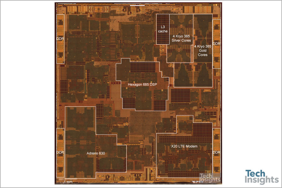
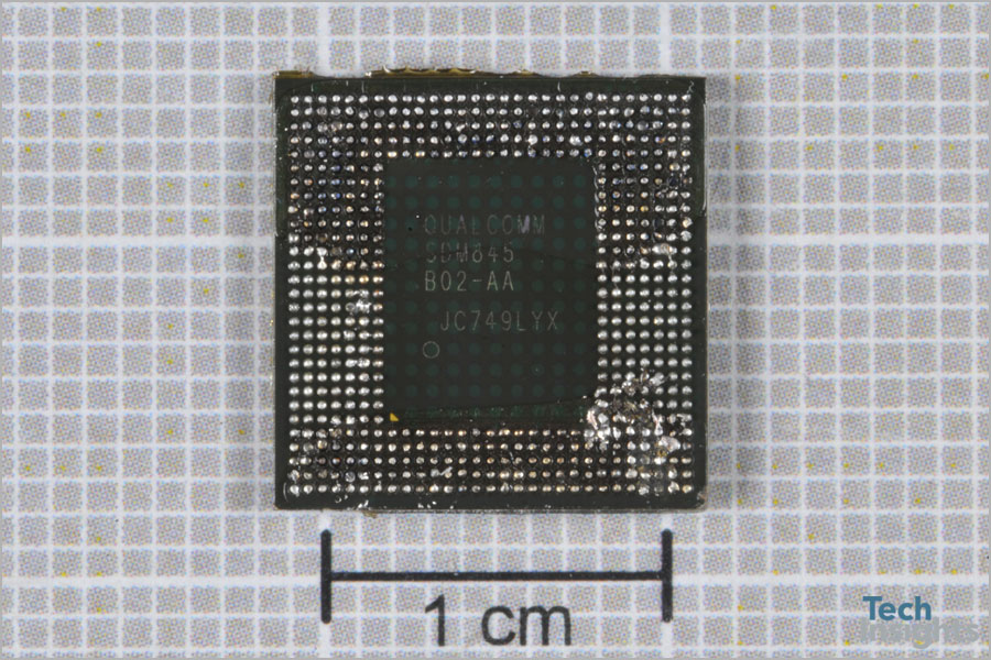
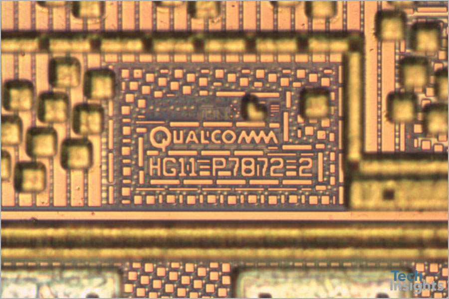
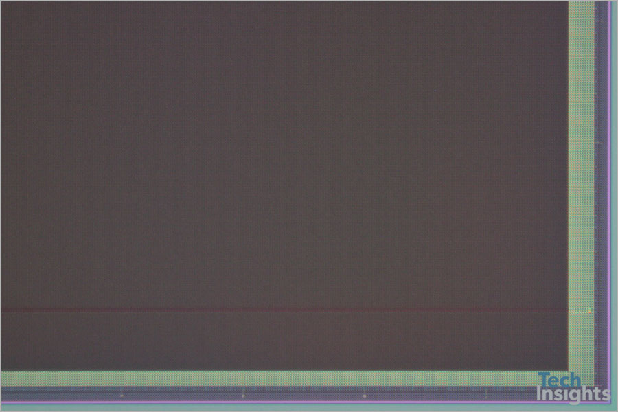
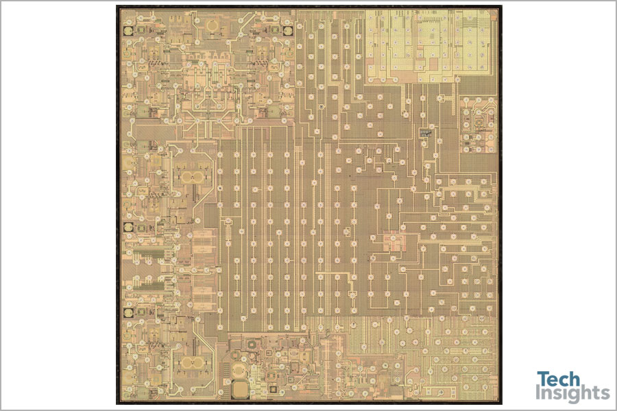
Qualcomm Snapdragon 845 Annotated Die Map
Qualcomm Snapdragon 845
We have decapped the Qualcomm-based Samsung Galaxy S9+ SM-G965U and can take a look into the latest updates to the Snapdragon flagship AP. Despite the heavy marketing of AI features, both the Snapdragon 845 and Exynos 9810 are software-based machine-learning solutions based on an SDKs, distributing workload to the CPU, GPU, or DSP based on requirements. Thus, as with the Exynos 9810, the main thrust for increased functionality is through increased CPU performance, with significant increases in area compared to Snapdragon 835, as well and increased customization of the ARM-based cores.
Both the Qualcomm and Samsung APs integrate similar class modems, both increased to the Cat. 18 download speed classification. Thus, as with the Samsung Exynos 9810 vs. the 8895, the Snapdragon 845 represents also an increased die size over the last generation 835, with a 30% increase in die size.
The Snapdragon 845 is overall 25% smaller than the Samsung 9810, for ostensibly the same specs and thus represents a lower cost solution. This fits the same trend as from the previous generation Samsung Galaxy S8. We noted a difference in memory usage as a key part of the difference AP die size difference. The functional block level analyses are in progress and we’ll see if this continues on the same pattern.
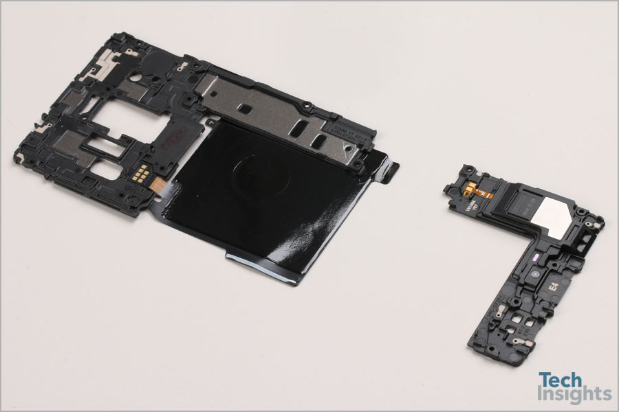
Samsung Galaxy S9+ Board Shots
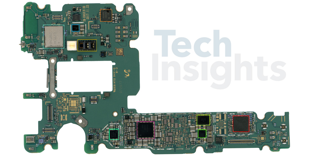
Samsung Galaxy S9+ Board Shot
-
Samsung 82LBXS2 NFC
-
Wifi Bluetooth Module
-
Heart Rate Sensor
-
Maxim MAX98512 Audio Amplifier
-
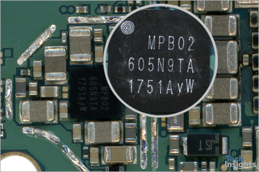
Samsung S2MPB02 Camera PMIC
-
Shannon 560 PMIC
-
Cirrus Logic CS47L93 Audio Codec
-
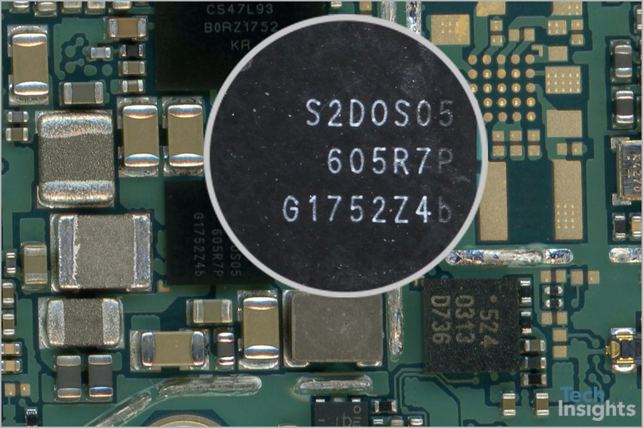
Samsung S2DOS05 Display Power Management IC
-
Shannon 965 RF Transceiver
-
Maxim MAX98512 Audio Amplifier
-
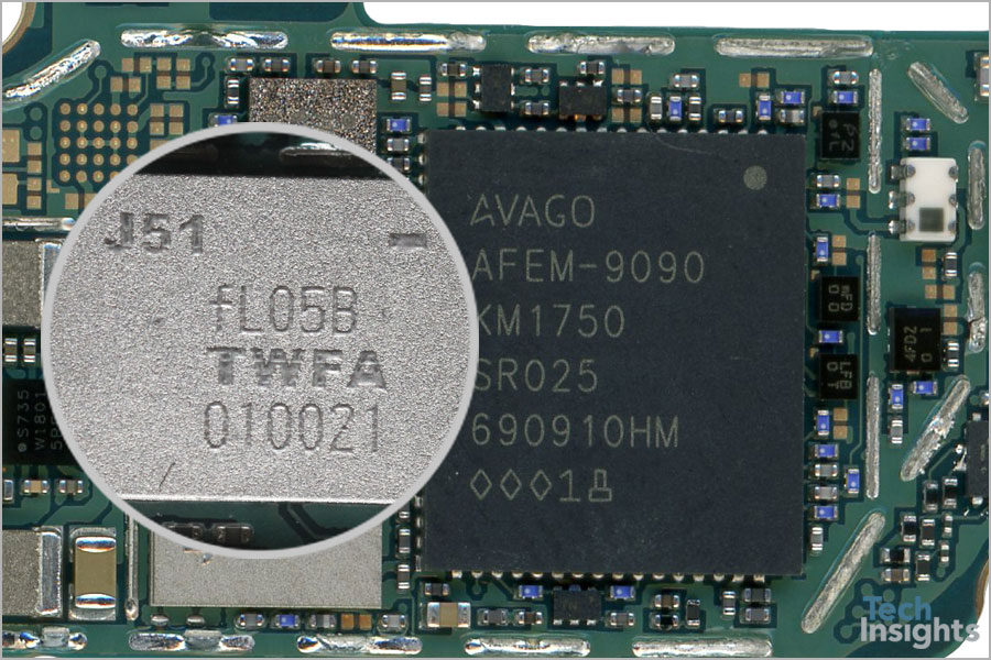
Avago AFEM-9090 Front End Module
-
Skyworks SKY77365-11 Power Amplifier Module
-
Murata fL05B Power Amplifier Module
-
Shannon 735 Envelope Tracker
-
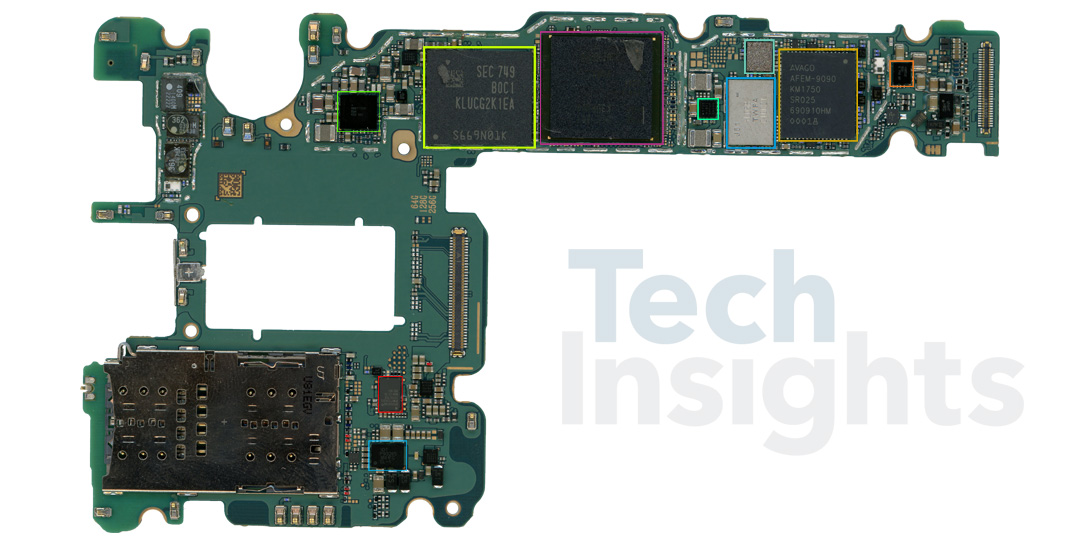
Samsung Exynos 9810 + Samsung 6 GB LPDDR4X (PoP)
-
Samsung KLUCG2K1EA-B0C1 NAND Flash
-
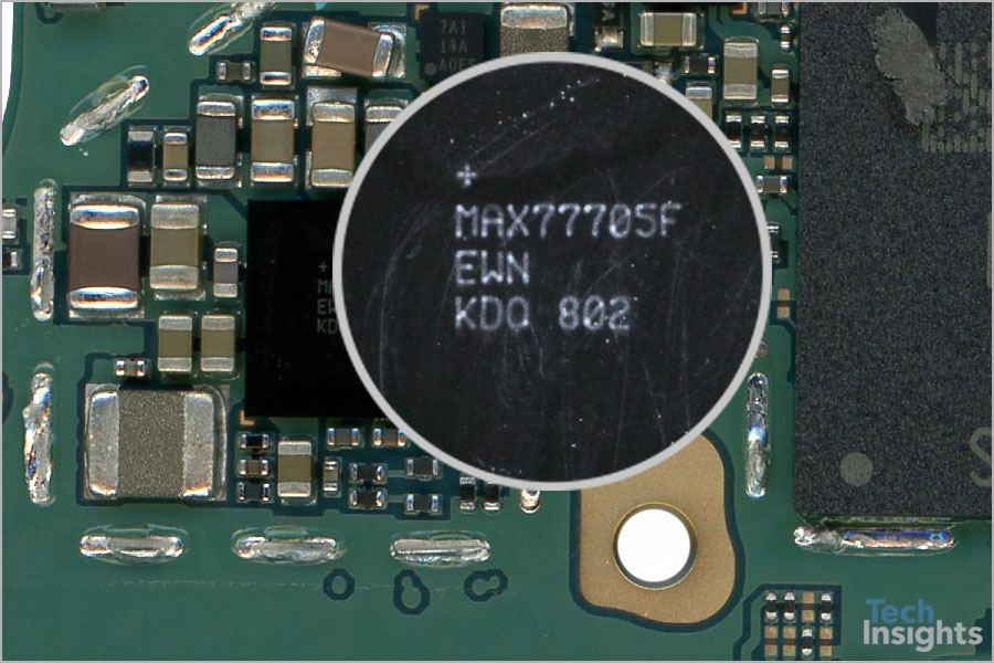
Maxim MAX77705F PMIC
-
Broadcom BCM47752 GNSS Receiver
-
IDT P9320S Wireless Charging Receiver
Costing
Here is a high-level view into the costs of the various components of the Samsung Galaxy S9+:
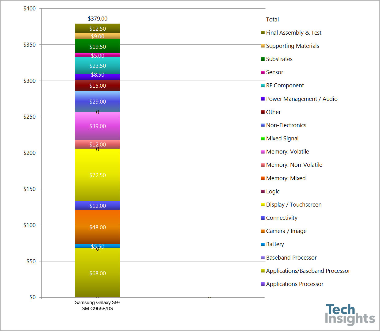
Samsung Galaxy S9+ Costing
* Costing note: All cost estimates provided here are compiled using information available to us at the time of the initial teardown. Some assumptions have been made where concrete data is not yet available. We will continue to gather and refine this costing data throughout our on-going deep-dive teardown process and analysis. While we do not expect drastic cost changes, we do expect some adjustments.
| Samsung Galaxy S9+ SM-G965F/DS Costs* | |
|---|---|
| Teardown Date | March-2018 |
| Applications/Baseband Processor | $68.00 |
| Battery | $5.50 |
| Camera / Image | $48.00 |
| Connectivity | $12.00 |
| Display / Touchscreen | $72.50 |
| Memory: Non-Volatile | $12.00 |
| Memory: Volatile | $39.00 |
| Non-Electronics | $29.00 |
| Other | $15.00 |
| Power Management / Audio | $8.50 |
| RF Component | $23.50 |
| Sensor | $5.00 |
| Substrates | $19.50 |
| Supporting Materials | $9.00 |
| Final Assembly & Test | $12.50 |
| Total | $379.00 |
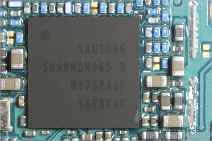
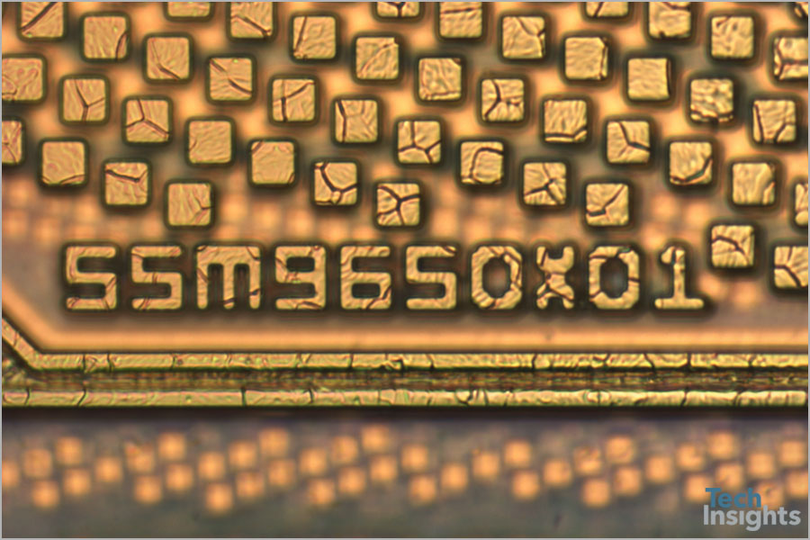
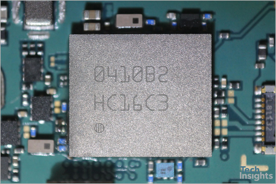
Samsung’s Shannon 965 RF Transceiver inside the Galaxy S9+
RF Transceiver
The Galaxy S9+ includes a new RF Transceiver, Samsung's Shannon 965. The Shannon 965 works with the LTE Cat.18 modem integrated in the Exynos 9810 to implement the 1.2Gbps download (peak) and 200Mbps upload (peak).
We now have the die photos of the Samsung Shannon 965 RF Transceiver, showing the die marking S5M9650X01. The die size (seal) is 5.96mm x 5.92mm = 35.28 mm2, slightly larger than the previous Shannon 955 RF Transceiver in the Galaxy S8.
Intel PMB9955 Baseband Processor
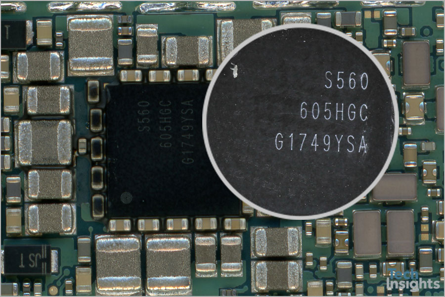
Power Management IC
Shannon 560, this is a new PMIC we have not seen before. For your reference, we saw a Shannon 555 PMIC in the Galaxy S8/S8+.
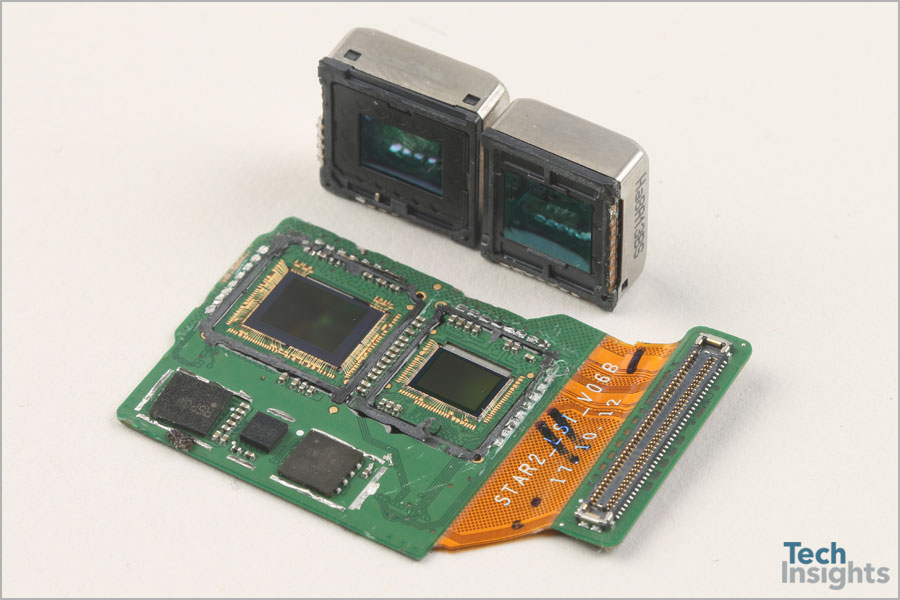
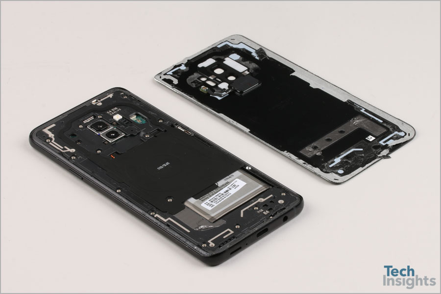
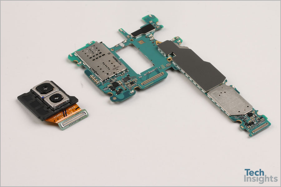
Camera Modules
Camera
Samsung claimed at MWC 2018 it had "completely re-imagined the camera" and built a phone around it. The Galaxy S9/S9+ design philosophy was to develop a camera system that can adapt to its environment, similarly to the human eye, and radically slow down time.
Today we can share our initial teardown images and have confirmed the iris scanner chip is new (compared to the S5K5E6YV used in the Note 7 and Galaxy S8). We are excited to analyze Samsung's new 3-stack ISOCELL Fast 2L3 and we'll be publishing updates as our labs capture more camera details. We also expect to purchase phones from other regions and confirm whether Samsung will continue to dual-source the main camera chip.
Galaxy S-series camera innovations recently disclosed by Samsung have contributed to the S9+ capturing top ranking in DxO Mark's mobile camera performance scoring system [1]. Samsung is not first to market with variable mechanical apertures or 3-layer stacked image sensors, however the integration of both elements in the S-series is a bold move to differentiate from other flagship phones. Subscribers to our ChipSelect IS service can look forward to Device Essentials projects on the new 3-layer stacked imager and new iris scanner chips. We have yet to confirm a dual-sourcing strategy for the wide-angle rear-facing camera, but we expect to find and report on a Sony 3-layer variant.
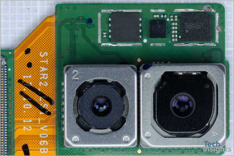
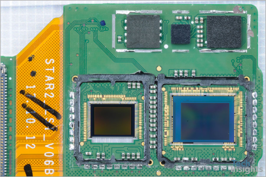
Dual Rear-Facing Cameras
Dual Rear-Facing Cameras
Sony led the evolution to 3-layer stacked imagers for smartphones beginning with its ISSCC 2017 paper in February 2017, followed by a product launch in April 2017 and more details coming in its IEDM 2017 paper [2,3]. Sony's first effort, which included a 1 Gbit DRAM, was in use in the Sony Xperia XZs which offered 6 s of slo-mo video based on 0.18 s of real time capture at 960 fps. Our analysis revealed a three-vendor solution for the IMX400: a Sony image sensor chip, a custom DRAM chip (including image sensor row control block) from Micron-Elpida and an image signal processor from TSMC.
Samsung recently announced its 3-die stacked ISOCELL imager at the pre-MWC 2018 Galaxy S9 event and with a formal press release for the Fast 2L3 following on Monday, February 26 [4]. The S9 wide-angle camera system, which integrates a 2 Gbit LPDDR4 DRAM, offers similar slo-mo video functionality with 0.2 s of video expanded to 6 s of slo-mo captured at 960 fps. Samsung promotes the memory buffer as beneficial to still photography mode where higher speed readout can reduce motion artifacts and facilitate multi-frame noise reduction.
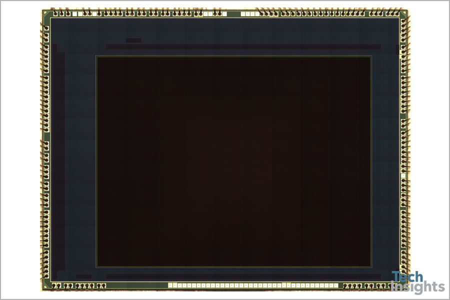
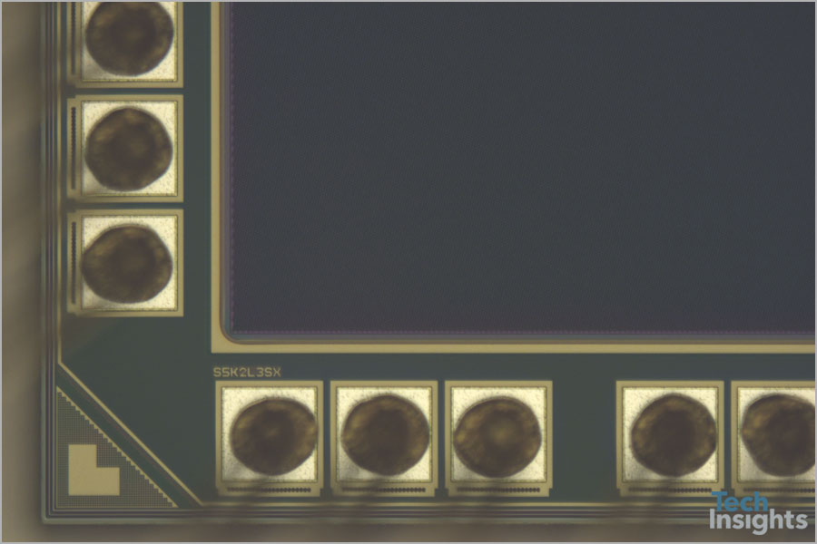
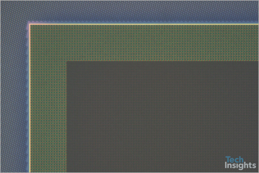
The wide-angle camera module uses Samsung's Fast 2L3, its third-generation 12 MP, 1.4 µm pixel pitch Dual Pixel ISOCELL sensor. The imager uses a Bayer RGB col-sm-12 col-lgor filter array, has die markings of S5K2L3SX and a die size of: 5.88 mm x 7.68 mm (45.2 mm2). Overall, that's a wider die than the S5K2L1 and S5K2L2, so we're anxious for our labs to produce die photos of the underlying die. The surface artifacts of through silicon vias (TSVs) are visible, and our cross-section work in progress will soon show the details of the 3-layer stack.
Samsung S5K3M3SM Die Photograph
The S9+ telephoto camera chip is a recycle of Samsung's 12 MP, 1.0 µm pixel pitch S5K3M3SM from the Galaxy S8. It's a two-die stacked imager with masked PDAF pixels, Bayer RGB col-sm-12 col-lgor filter array and die size of 4.21 mm x 5.61 mm (23.6 mm2).
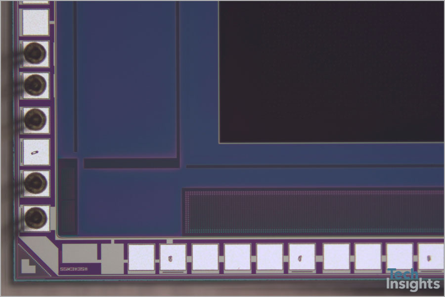
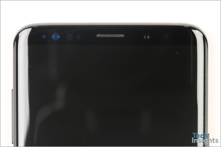
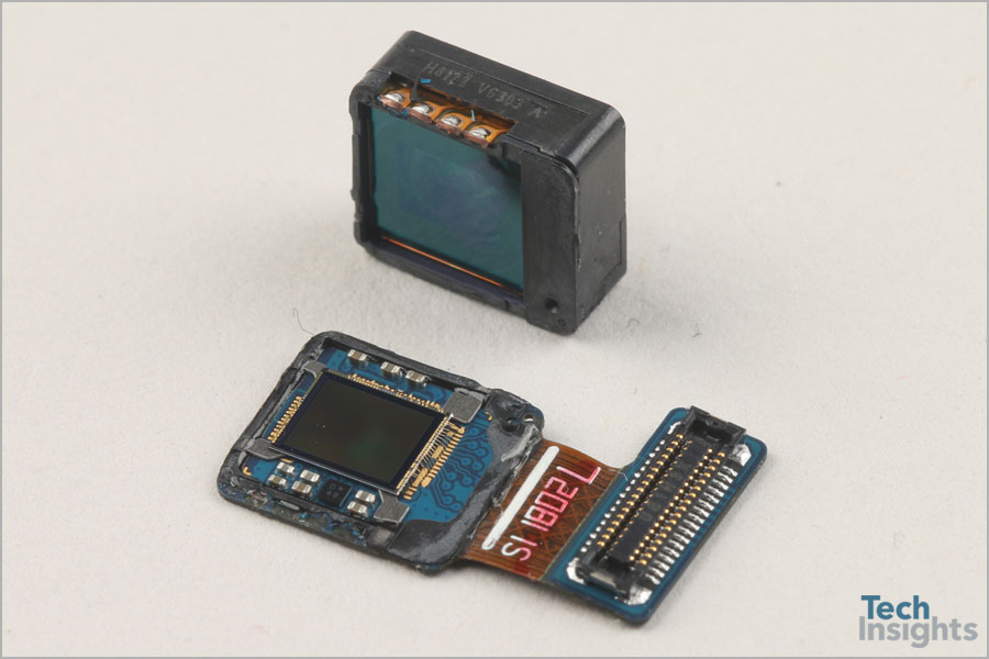
Front-Facing Iris Scanner
Front-Facing Iris Scanner
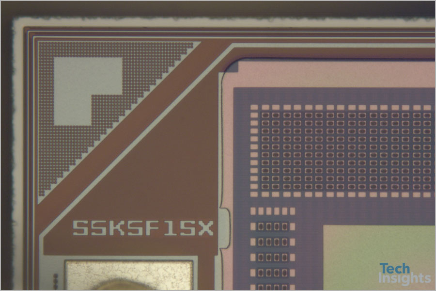
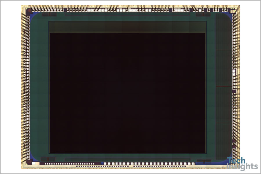
The S9's iris scanner is packaged in a 6.1 mm x 5.2 mm x 5.1 mm thick module. The monochrome, two-die stacked S5K5F1SX chip has a 6 MP resolution and 1.0 µm pixel pitch. This is a substantial upgrade from the up from the 5 MP resolution, 1.12 µm pixel pitch conventional back-illuminated sensor used in the Note 7/Galaxy S8. The S5K5F1SX die size is 3.11 mm x 3.78 mm (11.8 mm2).
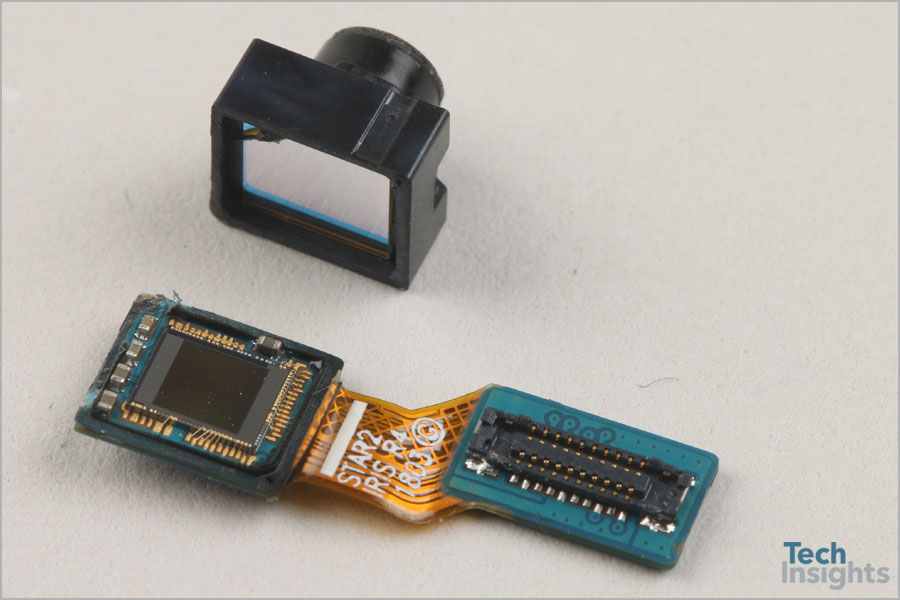
Front-Facing Camera
Front-Facing Camera
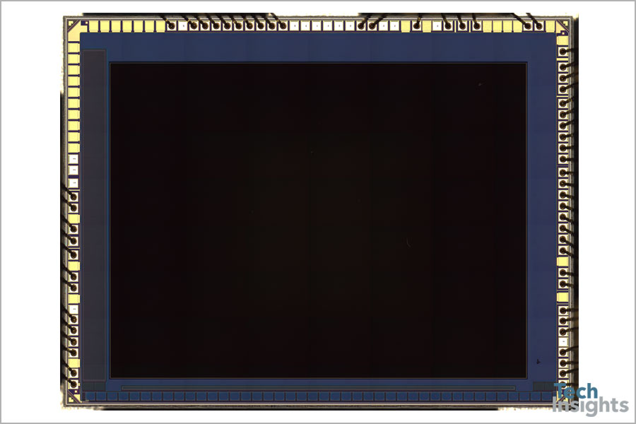
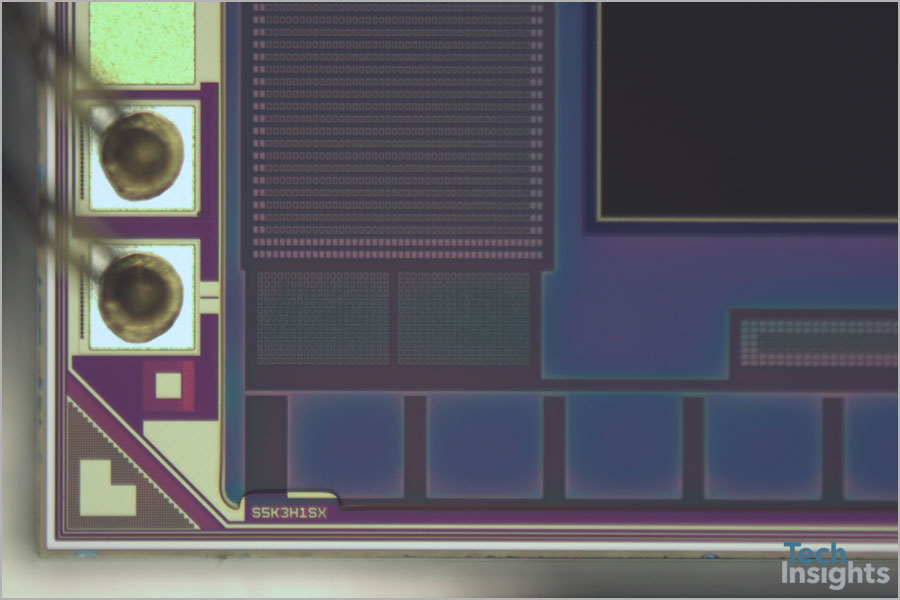
The Galaxy S9's front-facing camera chip is a recycle of the Samsung S5K3H1SX we first saw in the Galaxy S8. It's a two-die stacked imager with 8 MP resolution, 1.22 µm pixel pitch and a die size of 3.83 mm x 8.00 mm (30.6 mm2).
[1] https://www.dxomark.com/samsung-galaxy-s9-plus-review-premium-specs-top-end-performance/
[2] "A 1/2.3inch 20Mpixel 3-Layer Stacked CMOS Image Sensor with DRAM", Haruta, et al., ISSCC 2017
[3] "Pixel/DRAM/logic 3-layer stacked CMOS image sensor technology", Tsugawa, et al., IEDM 2017
[4] https://news.samsung.com/global/samsungs-newest-isocell-image-sensor-enables-mobile-devices-to-slow-down-time
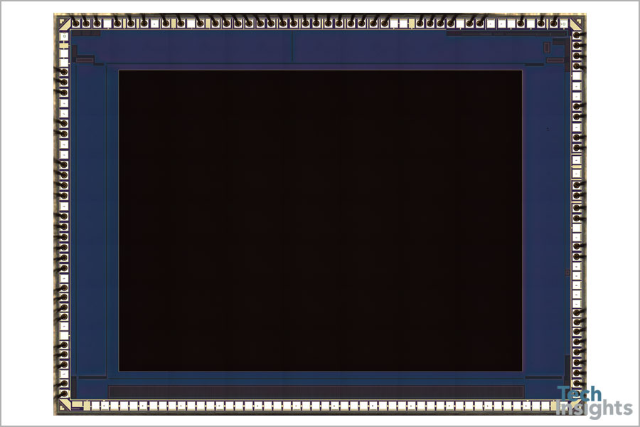
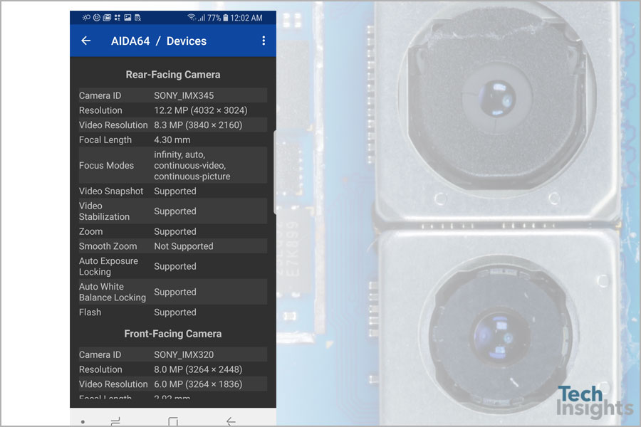
Sony IMX345
Camera Update! ~ March 15, 2018
We've just torn down a US-sourced Galaxy S9+, model SM-G965U, and as expected we learned Samsung is continuing its dual-sourcing strategy for the Galaxy S-series wide-angle camera chip. The IMX345 die size is 5.86 mm x 7.80 mm (45.7 mm2). The die dimensions are comparable to the sister Samsung S5K2L3SX chip and of course we're busy uncovering the details of both solutions, including the two other die stacked below these top image sensor chips. That's it for now - we wanted to share this fresh news and we'll be updating our IS subscribers with cross-sectional work in progress as it becomes available.
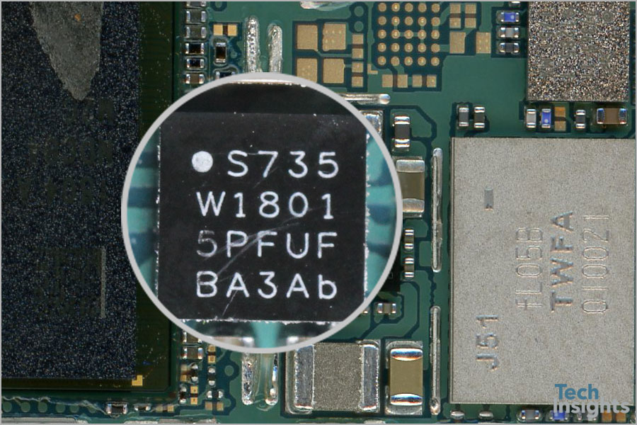
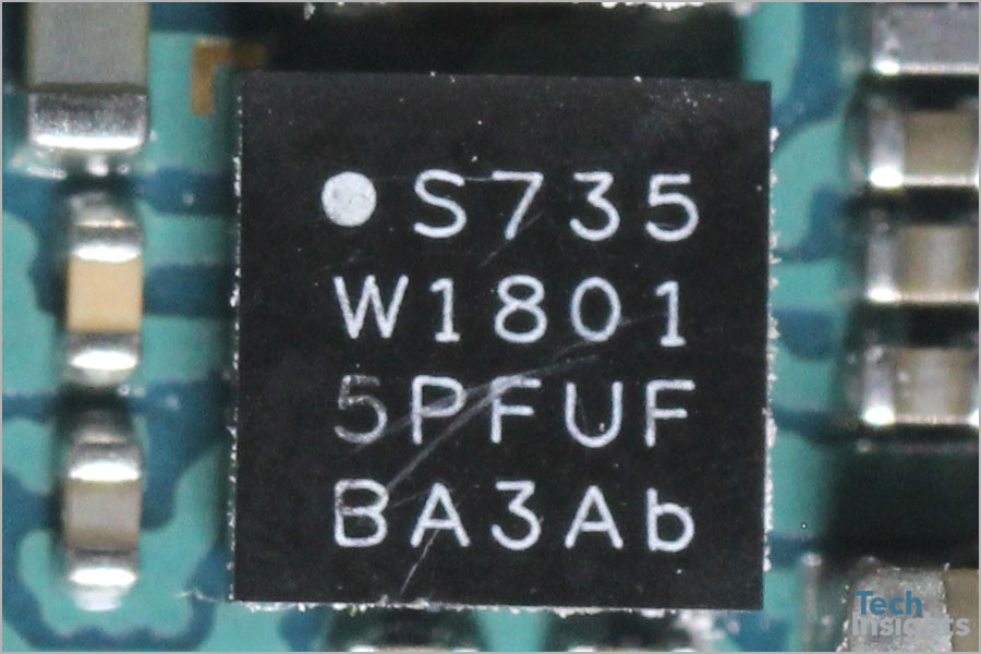
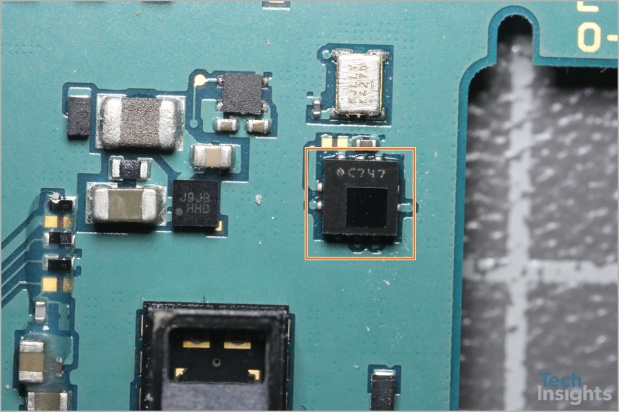
Shannon 735
Envelope Tracking
Shannon 735. We have seen it in many Samsung smartphones, such as Galaxy S8, S7, etc.
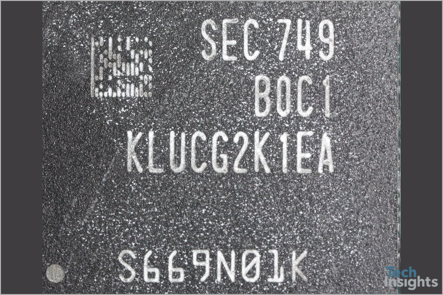
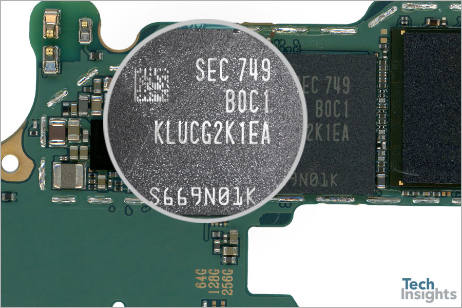
Samsung KLUCG2K1EA-B0C1
NAND Flash Memory
Samsung KLUCG2K1EA-B0C1, likely a 64GB UFS module.
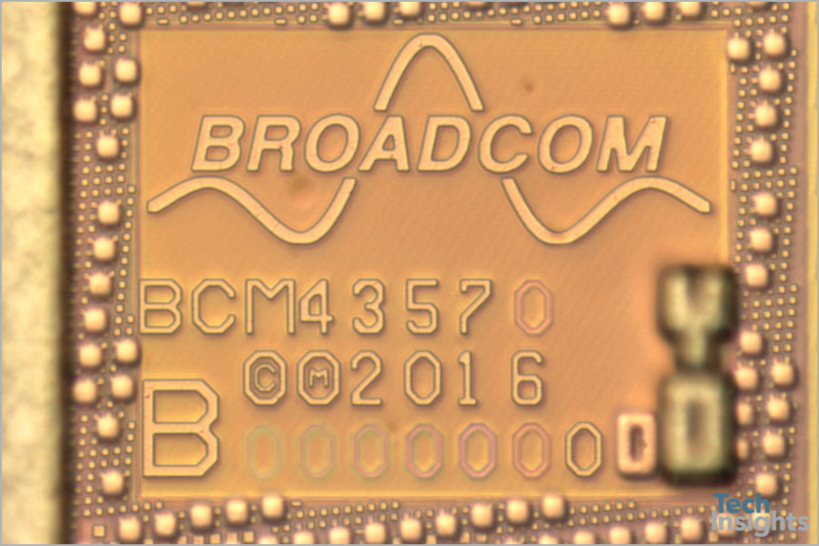
Broadcom BCM43570
Wi-Fi/Bluetooth
We have confirmed that the main wireless combo SoC die inside the above Samsung Electro-Mechanics module is Broadcom BCM43570, the same 802.11ac/Bluetooth 5.0 die we saw in the Galaxy S8.
NFC Controller
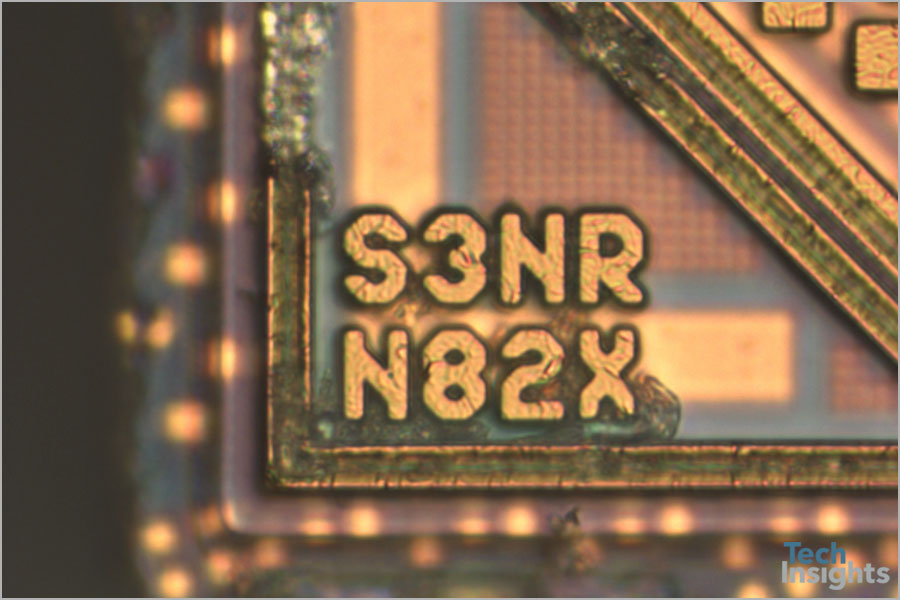
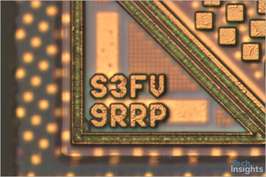
NFC Controller
Our decap has confirmed that the NFC controller is Samsung S3NRN82. We also found a Samsung Secure Element (SE) die S3FV9RRP in the NFC module. For your information, the same SE socket in the Galaxy S8 was from STMicroelectronics.
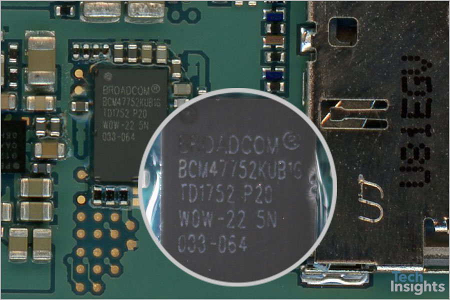
Broadcom BCM47752 GNSS receiver
GNSS
We found a Broadcom BCM47752 GNSS receiver with integrated sensor hub.
A side note: we had been hoping to find Broadcom’s BCM47755 - which supports two frequencies (L1+L5), compared to the legacy chip’s L1 – but the Samsung Galaxy S9+ does not include this part. We will continue our hunting. According to Broadcom, the BCM47755 can achieve lane-level accuracy outdoors and much higher resistance to multipath and reflected signals in urban scenarios, as well as higher immunity to interference and jamming.
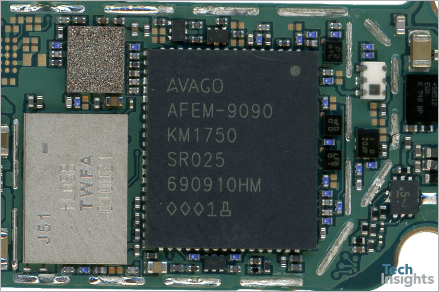
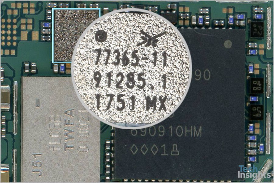
Power Amplifiers and Front-Ends
Power Amplifiers and Front-Ends
There is a new Broadcom (AFEM-9090) Front-End Module which looks to support both the high- and mid-cellular bands. This means there was a design win change from the Samsung Galaxy S8 SM-G955F in that Qorvo is no longer supporting any cellular bands in the “F” model of the new Samsung S9+. We will have to see if this is true in the Qualcomm S9+, or if this design change is across all variants for the new Galaxy S9 product line.
What we have found in the Galaxy S9+:
- Avago AFEM-9090 Front-end Module
- Skyworks SKY77365-11 Power Amplifier Module (PAM) for Quad-Band GSM/GPRS/EDGE
- Murata fL05B Power Amplifier Module
MEMS Sensors
MEMS Sensors
STMicroelectronics has won the MEMS Accelerometer & Gyroscope (LSM6DSL inertial module) and pressure sensor (LPS22HB) sockets, same design-wins as we saw in the previous Galaxy S8/S8+ phones.
Power Amplifiers and Front-Ends
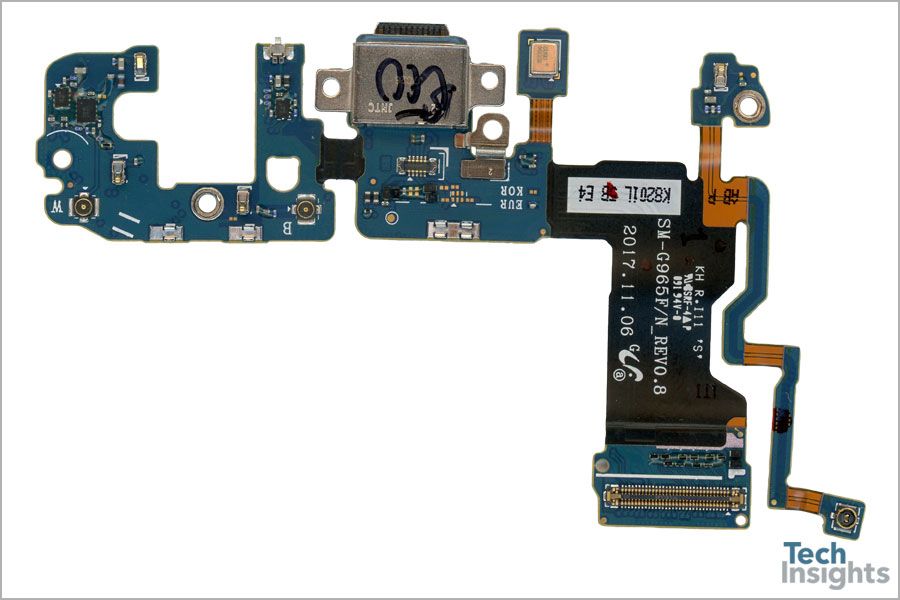
MEMS Microphones
On the main board we found two Knowles MEMS microphones, and a third Knowles MEMS microphone on the USB-C flex board. We noted on the USB-C flex board the markings “EUR” and “KOR” suggesting there is a different flex assembly for other Galaxy S9 models for other regions.
This makes sense since this particular substrate assembly has many of the cellular antenna contacts. We did not find the same pronounced markings on last years Galaxy S8 models.
AKM AK09916 electronic compass
Electronic Compass
AKM wins the 3-axis electronic compass socket again. It is the same AK09916 as we saw in the Galaxy S8.
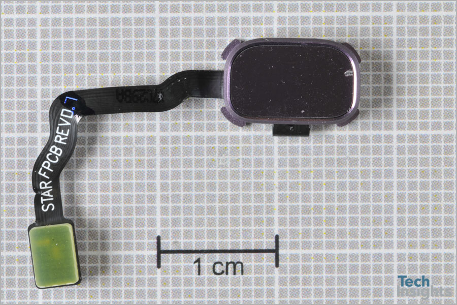
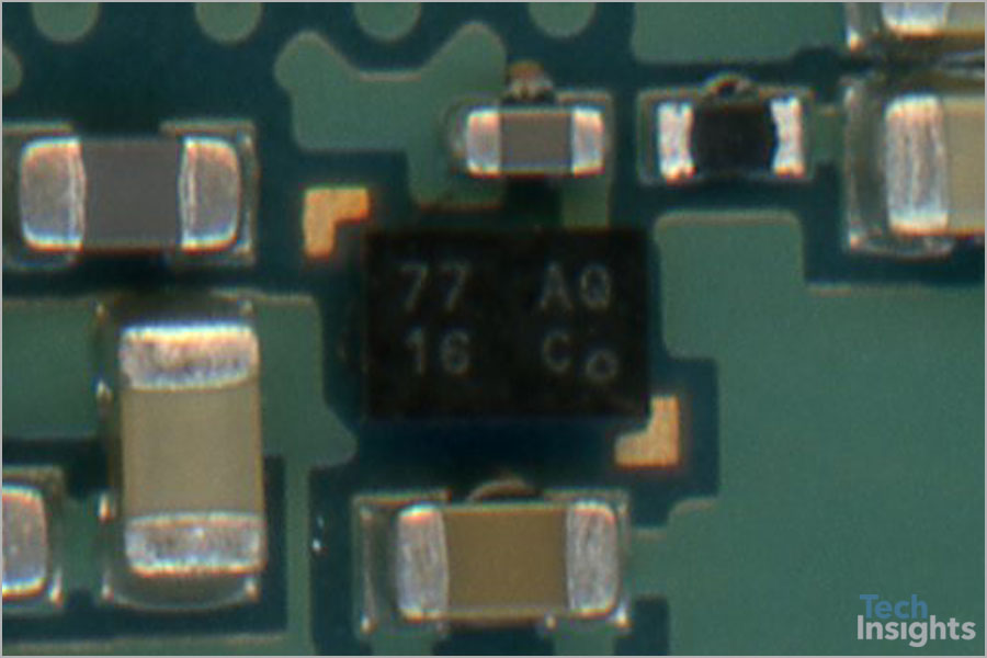
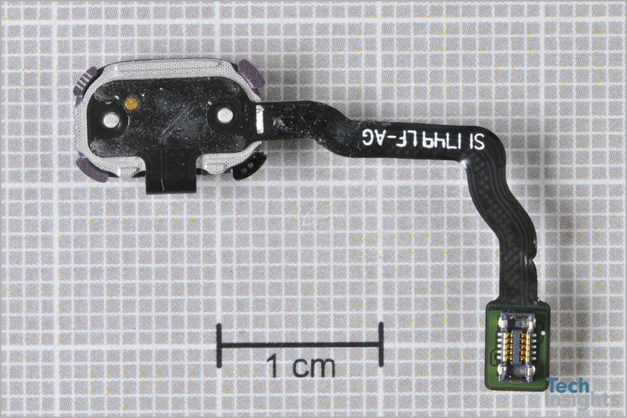
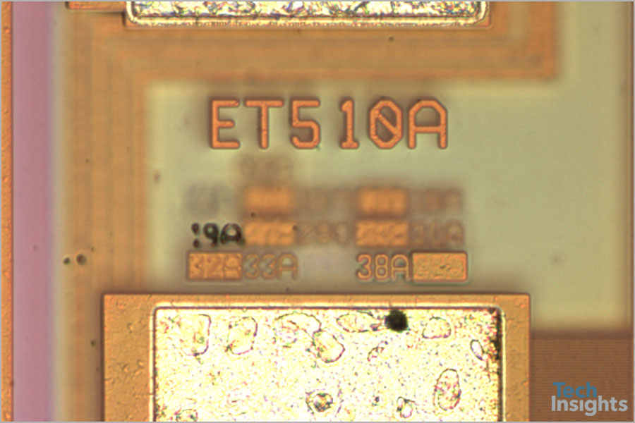
Egis Technology’s fingerprint sensor
Fingerprint Sensor
Biometric identification is a very important feature of today’s smartphones. The Samsung Galaxy S9+ combines face recognition, iris scan, and fingerprint sensor. We decapped the module to further explore the fingerprint sensor, and to our surprise we found that Taiwan’s Egis Technology has won the fingerprint sensor socket. This means a socket loss for Synaptics which had been the fingerprint sensor supplier of Samsung’s flagship Galaxy S series phones from the S5 to the S8.
As a side note, there are mainly 3 kinds of fingerprint sensor solutions for smartphones: capacitive fingerprint sensor, ultrasound, and optical.
The most popular one is the capacitive fingerprint sensor. For example, Apple’s TMDR92 used in the iPhone 5S, 6, and SE, TMFK67 used in the iPhone 6s, iPhone 7 fingerprint sensor, Fingerprint Cards FPC1155, Goodix GF5118M. These are all capacitive fingerprint sensors.
The second one is the ultrasound solution. For example, Qualcomm Snapdragon Sense ID.
The third one is the optical fingerprint sensor solution targeting the full screen smartphones. With smartphones trending toward larger screens with higher screen-to-body ratios, a fingerprint sensor located on the front will definitely affect that ratio.
We have recently purchased the Vivo X20 Plus UD smartphone, the world’s first in-display fingerprint sensor phone based on Synaptics’ optical fingerprint sensor, and we are analysing it now. As we are expecting to see more design wins in this year’s Android phones, we are unsure at this time why Samsung did not select the Synaptics optical fingerprint sensor in the Galaxy S9+.
Before the Android world’s facial recognition and ultrasound fingerprint sensor solutions mature, in-display optical fingerprint sensor solutions seem to be the best option for full screen smartphones to compare to Apple’s Face ID. At MWC18, Vivo revealed its APEX™ FullView™ concept smartphone, featuring world’s first half-screen in-display fingerprint sensor.
It looks that the fingerprint sensor market will continue to see innovations, and we are looking forward to seeing new products in this area.


