Apple iPhone 5s Teardown
Posted: September 20, 2013
Contributing Authors: Jim Morrison, Ray Fontaine, Dick James and Chad Davis
Inside
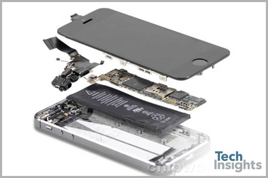
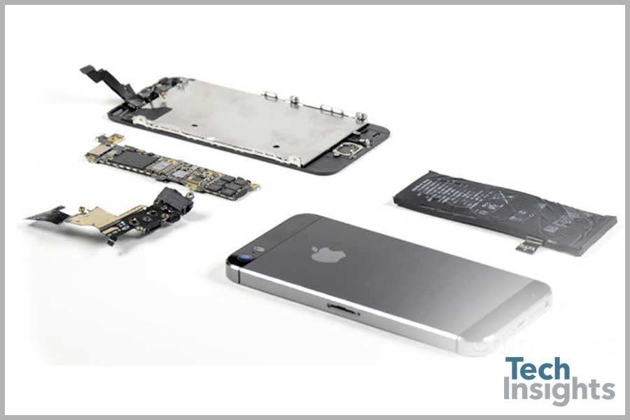
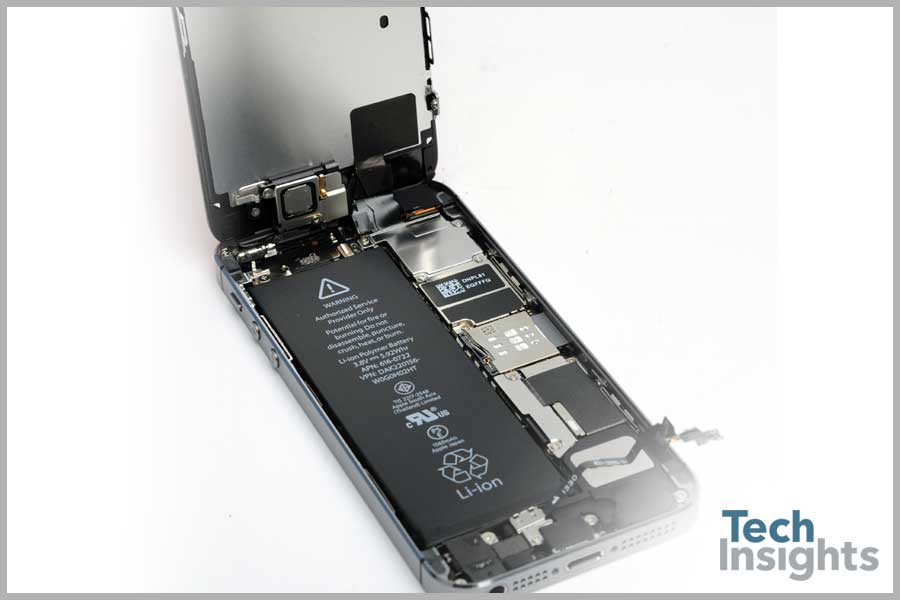
On September 10, 2013, Apple announced two new iPhones, the 5s and 5c. Since the announcement, we at TechInsights have been anxiously waiting for the opportunity to get our hands on the devices. Phone in-hand, we did what any self-respecting technology company would do - destroy it (carefully). Follow us along today as we dive into what's new and exciting this time around, including the A7 64-bit ARM CPU and the mysterious M7 motion co-processor, as well as estimated bill of materials.
Board Shots

Front Board
Front Board
- Apple A7 processor / Elpida LPDDR3 (1 GB)
- NXP LPC18A1 “M7” Coprocessor
- Qualcomm MDM9615M Modem
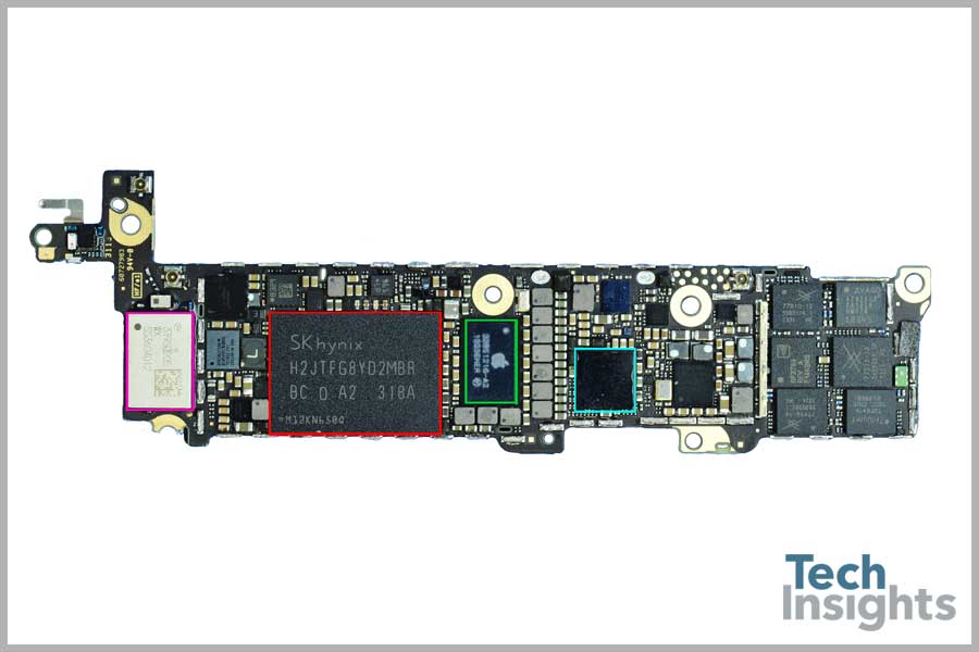
Back Board
Back Board
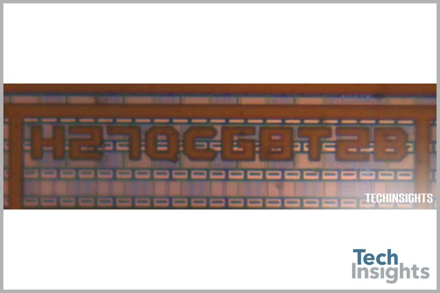
- Hynix 64 GB NAND Flash, Package Mark: H2JTFG8YD2MBR, 8 stacked NAND Flash, Die Mark: H27QCG8T2B
- Apple Logo, Package Mark: 338S1216-A2, Die Mark: Dialog D2045
- Murata Combo Radio MCM, Package Mark: 339S0205, Die Mark:Broadcom BCM43342
- Apple Logo, Package Marking 338S11201, Cirrus Logic, Die Mark: CLI1G009A1
Apple iPhone Cost Estimate
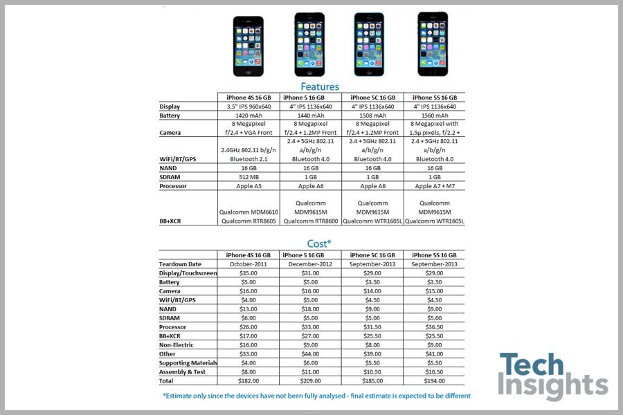
Apple iPhone Cost Estimate

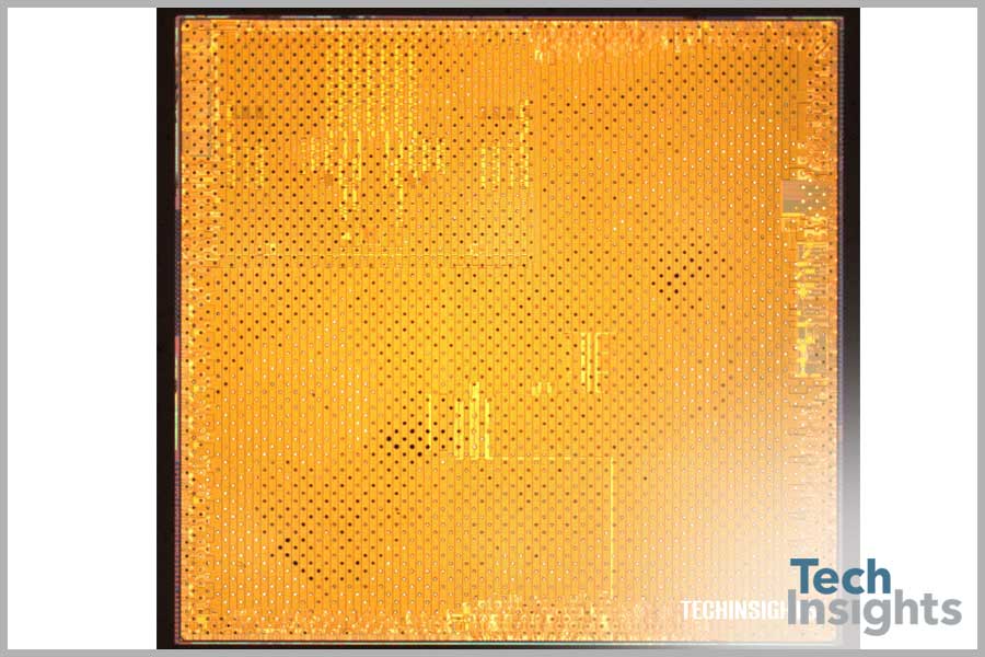
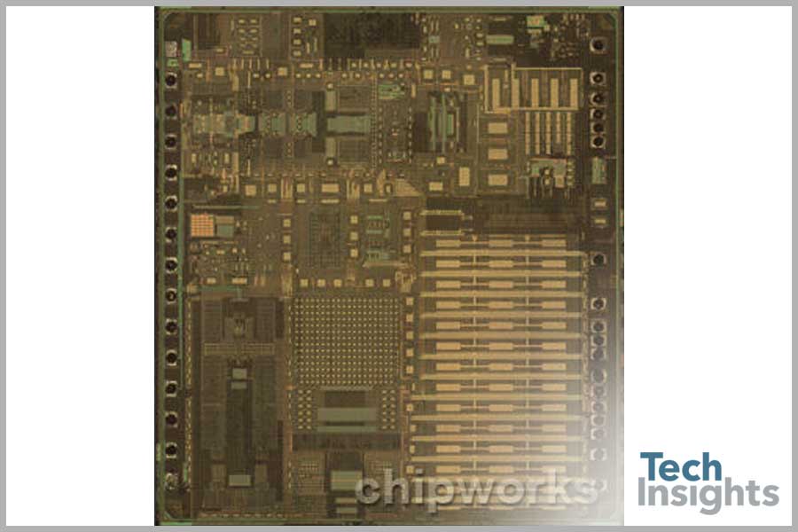
The A7 Processor
The A7 Processor
The processor this time around is Apple’s new A7, a 64-bit system-on-chip ARM.
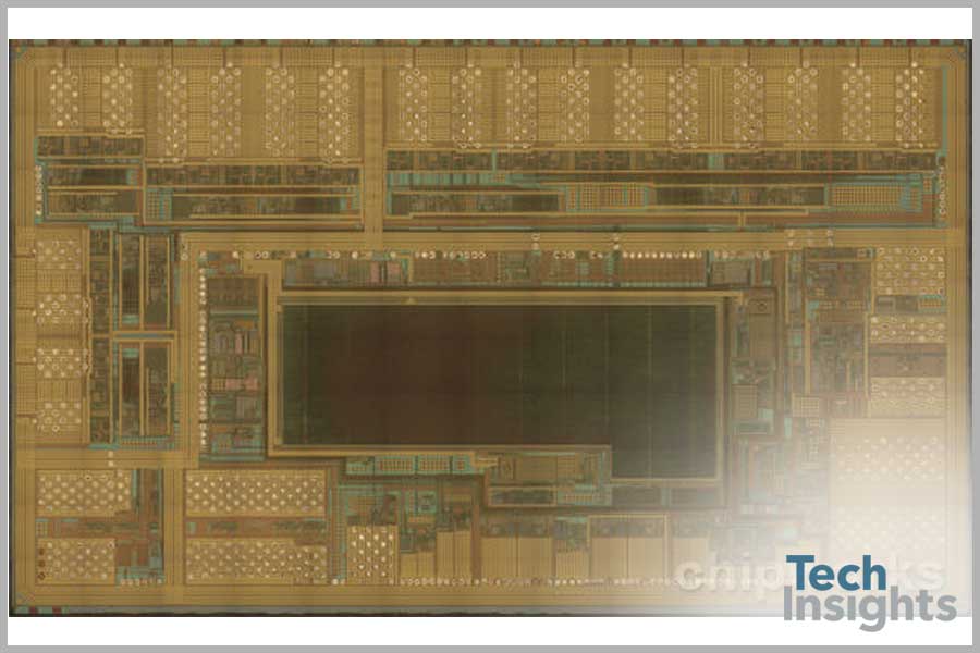
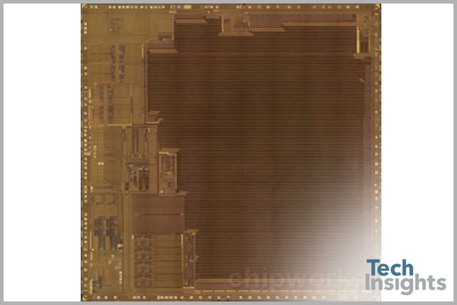
We have confirmed through early analysis that the device is fabricated at Samsung’s Foundry and have confirmed the process type and node in the next section. External die, package photo, top metal die photo and package markings shown below. The last picture... drum roll... Transistor Level Die Photo.
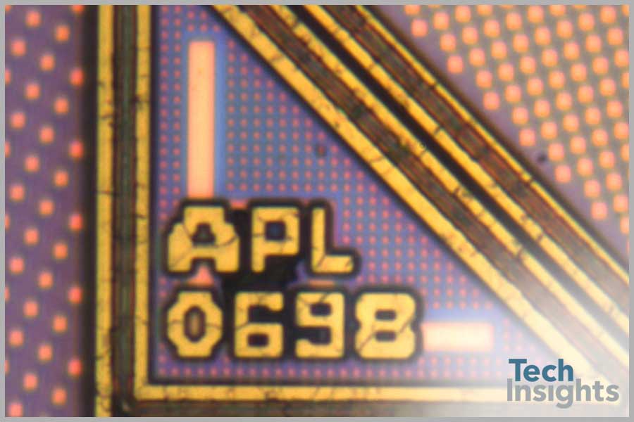
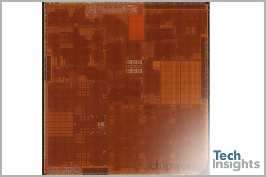
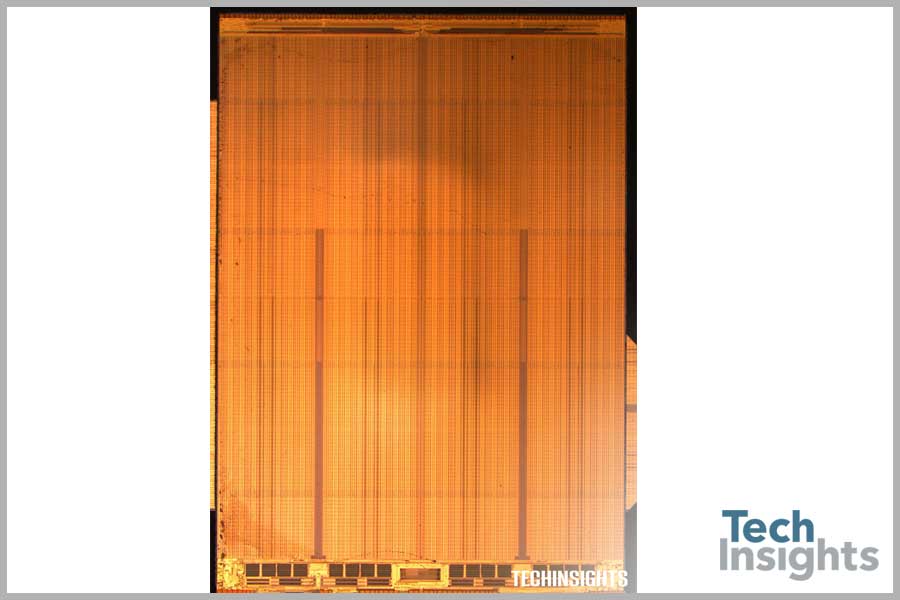
The A7 does use Samsung’s 28-nm process
Earlier in the day we established from the look of the die that the A7 was manufactured by Samsung. In the meantime our guys have been grafting away in the lab, and came to the “boring” conclusion that the chip looked exactly the same as the last one. The devil is in the details, however, and we have to do some measurements to see the difference.
Below is an electron microscope image of a cross-section of a group of transistors in the A6 (APL0598) chip, fabbed in the Samsung 32-nm high-k-metal gate (HKMG) process. For convenience we have measured ten, so the dimension of the “contacted gate pitch” (a standard industry measure) is 123 nm.
Now if we look at a similar image of the A7 (APL0698), and we see that the contacted gate pitch is 114 nm. So, even allowing for measurement error (we figure +/- 5nm), we’re pretty sure that we see a shrink, and that the A7 is made on the same process as the new Samsung Exynos 5410, the 28-nm HKMG process. That doesn’t sound much, a mere 4 nm, but again if you do the math and remember that we’re talking area shrink, not linear dimensions, then 28^2 divided by 32^2 (784/1024) comes out at about 77% of the area for the equivalent functionality. Or, given that the A7 is 102 mm^2 compared with 97 mm^2 for the A6, more functions in a slightly bigger area.

A7

A7

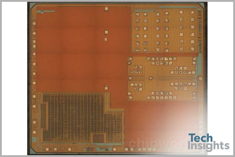
M7 Co-Processor
The M7 Co-Processor
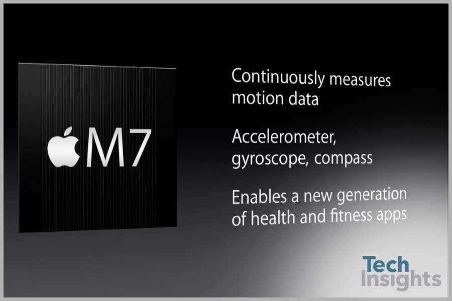
The M7 is a new direction for Apple - in an effort to reduce power consumption, the M7 chip is dedicated to collecting and processing accelerometer, gyroscope and compass data. That being said, The M7 has been a difficult chip to locate on the board and rumors have been going around about the lack of a discrete M7 chip inside the iPhone 5s. All expectations up to now were pointing to a stand-out chip as seen below at the Apple Town Hall event.
Luckily, we’ve been able to locate the M7 in the form of the NXP LPC18A1. The LPC1800 series are high-performing Cortex-M3 based microcontrollers. This represents a big win for NXP. We had anticipated the M7 to be an NXP device based on input from industry analysts and our partners and we are happy to see this to be the case.
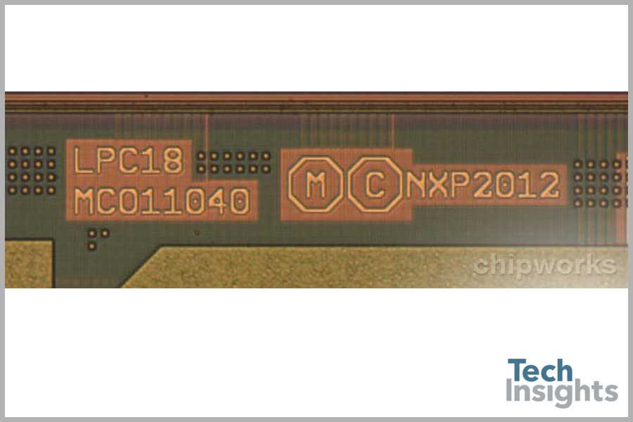
We did some poking around on the NXP website, looking at their LPC range of products; and we couldn't find any specific part that matched the look of the LPCA1, particularly the 30-ball WLCSP packaging. So we've come to the tentative conclusion that this is likely a customised LPC18xx chip built for Apple, similar to those we've seen from Dialog and Cirrus over the years (A1 stands for Apple-1?).
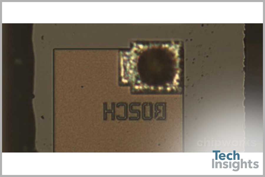
The M7 is dedicated to processing and translating the inputs provided to it by the discrete sensors; the gyroscope, accelerometer and electro magnetic compass mounted throughout the main printed circuit board. Traditional Apple techniques lead us to believe that these discrete sensors are STMicroelectronics for the accelerometer and the gyroscope while the electro magnetic compass would again be an Asahi Kasei Microdevices (AKM). We have since confirmed the compass to be AKM’s AK8963 and the gyroscope to be STMicroelectronics. But to our surprise the accelerometer is actually a design win for Bosch Sensortech with their BMA220 3-axis accelerometer (the first Bosch we've ever seen in an Apple product). We dive deeper into the M7 and its children in the next section.

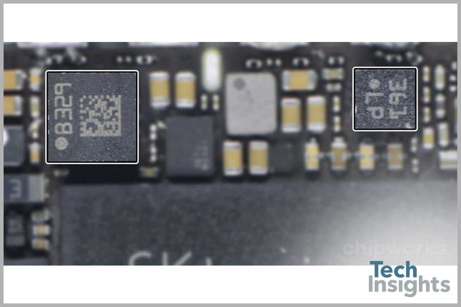
M7's children
The M7's children; a 3-Axis Accelerometer, a 3-Axis Gyroscope and a Compass IC
The previously unknown MEMS devices that had us so interested when we first cracked open the iPhone 5s one with markings B361LP and another B329.
The first is a 3-Axis Accelerometer. Based upon the die markings observed in the 2mm x 2mm device, the first unknown MEMS device has been ID’d as a Bosch Sensortech BMA220 3-axis accelerometer. This is the first time in our experience looking at Apple products that we see a Bosch MEMS device included. Previously this has been a socket dominated exclusively by STMicroelectronics. Great socket win Bosch!
The second is a 3-Axis Gyroscope. This device with package markings B329 has been identified as an STMicroelectronics 3-axis gyroscope, as expected.
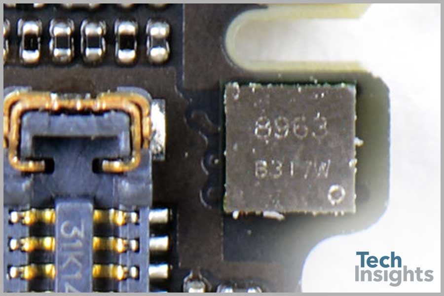
Holding the compass socket for another round is AKM’s AK8963 3-axis electronic compass IC. The AK8963 combines a magnetic sensors to detect X, Y, and Z axis, a sensor driving circuit, arithmetic circuit and signal amplifier chain.

Cameras
The Cameras
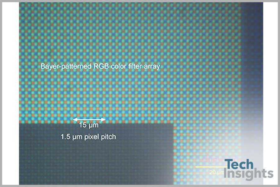
Which is preferable, more pixels or a sensor with higher sensitivity? We all would like to have both, however at some point camera system and chip designers have to turn the knob towards one or the other. Apple has opted to stand on an 8 Mp resolution for the 5S iSight camera, but have increased the active pixel array area by 15%. With the help of a larger f/2.2 aperture, the system delivers a 33% increase in light sensitivity.
The iSight camera has DNL markings which are consistent with the markings on the camera modules housing the Sony IMX145 we saw in the iPhone 5 and 4s. The iPhone 5S 8 Mp iSight camera module is 8.6 mm x 7.8 mm x 5.6 mm thick. The new iSight camera module has been refreshed with a custom 1.5 µm pixel pitch stacked (Exmor-RS) Sony sensor.
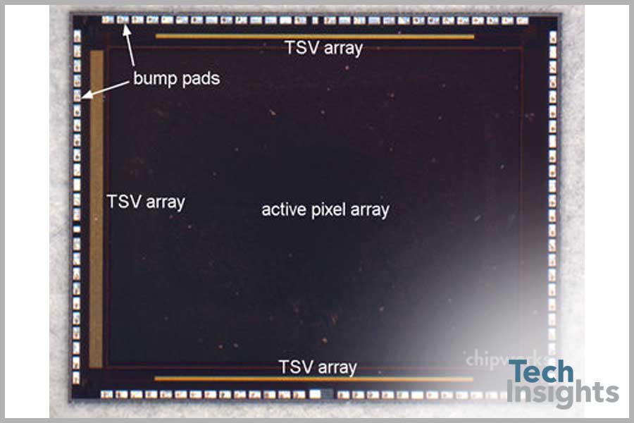
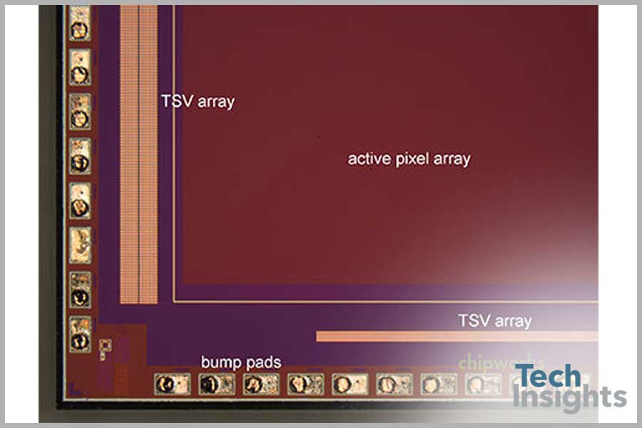
The side-view X-ray image shows us what is now conventional packaging for Apple’s iSight cameras: a ceramic chip carrier with a back-mounted, back-illuminated CMOS image sensor (CIS) chip. Bump bonding is used to connect the die signal pads to the chip carrier lands.
A decap and quick peek through our microscope shows the telltale signs of a Sony Exmor-RS sensor. We first saw Sony’s stacked CMOS image sensor chips (using through-silicon vias -TSVs) in the 8 Mp ISX014 from a Fujitsu tablet, and then in the 13 Mp IMX135 from the Samsung Galaxy S4 primary camera (The CIS is stacked on the image signal processor - ISP).
We’ve confirmed that the FaceTime camera chip is fabricated by OmniVision.
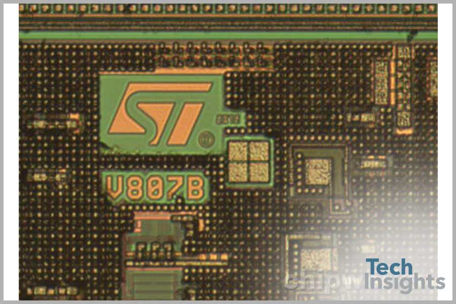
Power Management IC
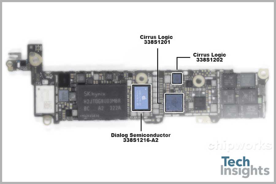
New Power Management IC and a new audio codec and class D amplifier
As we mentioned earlier, we’re seeing a lot of familiar components inside the iPhone 5s. The major standouts being the new A7 processor and two new MEMS devices. We are also seeing a new power management IC by Dialog Semiconductor and a new audio codec and class D amplifier by Cirrus Logic. The Power Management IC by Dialog Semiconductor has the part number 338S1216-A2. The new parts by Cirrus are numbered as 338S1202 for the Class D audio amplifier and 338S1201 for the Audio Codec. Note that the audio codec is ~30% smaller than the codec inside the iPhone 5.
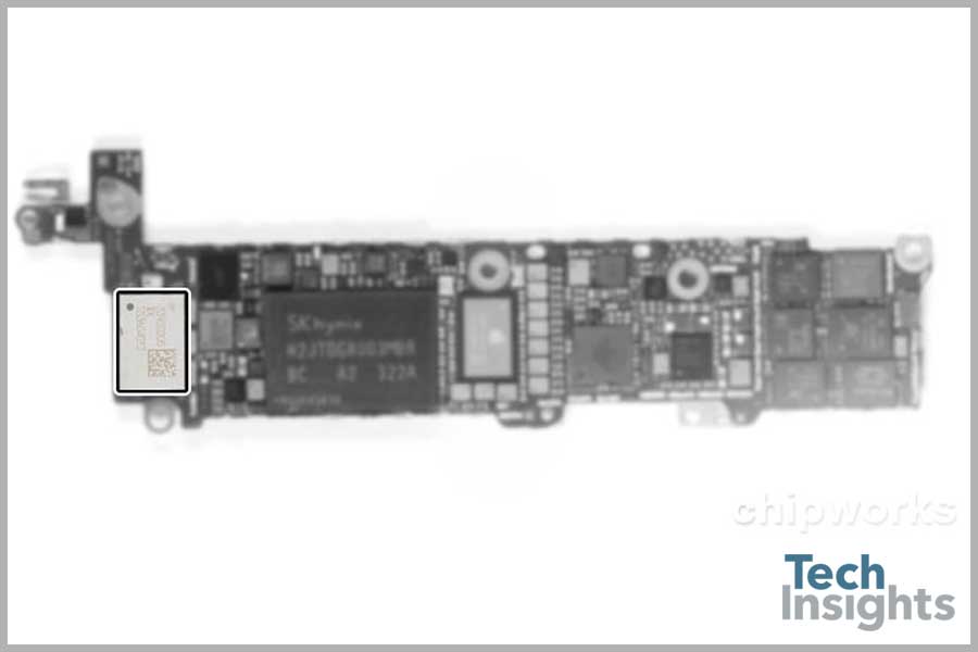
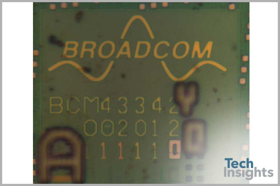
Wi-Fi SoC
The Wi-Fi SoC
Contained within this module is the BCM43342. This specific die, we have not seen before. The iPhone 5 and several other smartphones on the market employ the BCM4334. The Broadcom BCM4334/BCM43342 is a single chip device with integrated IEEE 802.11 a/b/g and single-stream IEEE 802.11n MAC/baseband/radio, Bluetooth 4.0, and FM radio receiver. It is designed to be used with external 2.4 GHz and 5 GHz front-end modules, which include power amplifiers, T/R switches and optional low noise amplifiers.
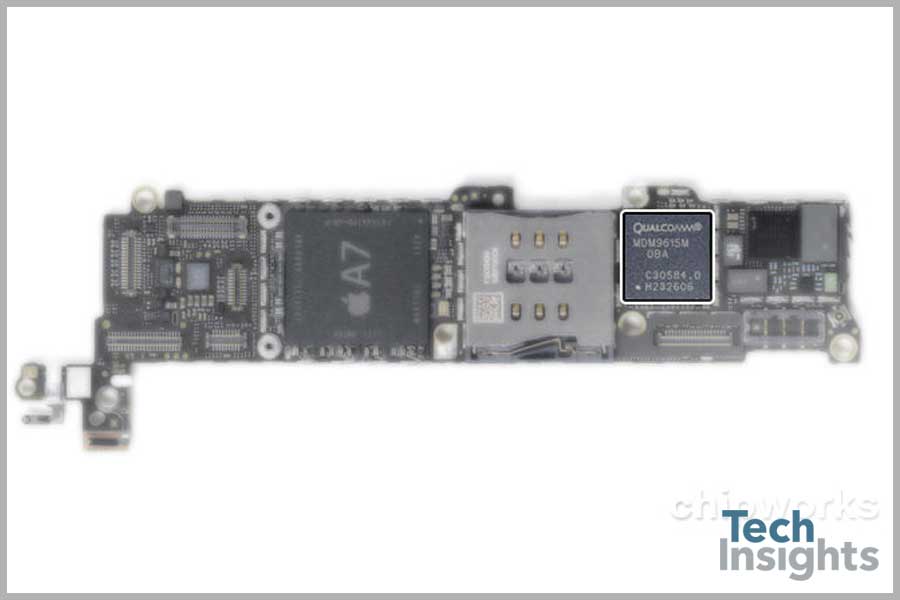
Qualcomm MDM9615M 4G LTE Modem
The 4g LTE Modem by Qualcomm
Here we have the Qualcomm MDM9615M 4G LTE modem. This device utilizes a two-chip solution in the form of a Samsung DRAM to retain carrier specific information and a Samsung-fabricated LTE baseband processor. This has been quite a a popular option recently as we’ve seen this device in over a dozen unique smartphones this year alone.

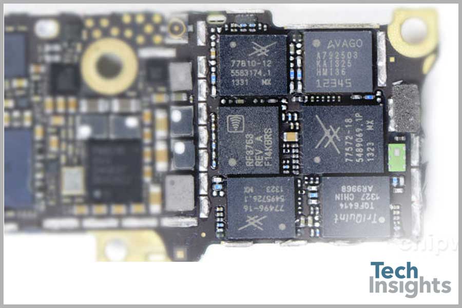
RF and PA Design Wins
The RF and PA Design Wins
The chips that deliver the RF capabilities of a phone tend to be over shadowed by more consumer-friendly specifications like the number of GB of storage, or the clock speed of a processor. However, they are critical to the user experience of the device. Because of the nature of radio frequencies, they also require a complex number of different components to work together in harmony – or more accurately, without interfering with one another. Our friends at Barclays have done a thorough job at identifying the RF design wins inside the iPhone 5s:
- RF Micro RF3763 Power Amplifier-Duplexer (PAD) for B5 / 8 Dual PAD
- Skyworks SKY77572 Band 18/19/20 Power Amplifier Device
- Skyworks SKY77810 2G/EDGE Power Amplifier Module
- Avago A792503 Band 25/3 Power Amplifier Device
- Skyworks SKY77496 Band 13/17 Power Amplifier Device
- TriQuint TQF6414 Band 1/4 Dual Power Amplifier Device

Elpida LPDDR3
DRAM Design Win - Elpida LPDDR3
Although Elpida’s published part decoder doesn’t include LPDDR3 devices, the ‘F’ prefix should indicate the product family as LPDDR3 (a ‘B’ would indicate LPDDR2). The remainder of the number confirms the use of 4 Gb chips - with two chips in the memory package.

Hynix 64 GB E2NAND
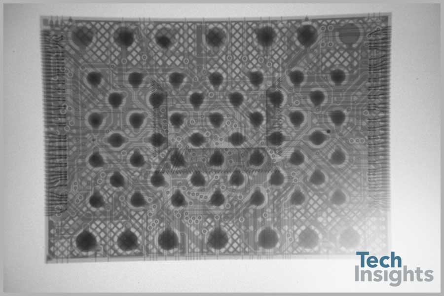
Flash Design Win – Hynix 64 GB E2NAND 3.0
The NAND flash memory on the iPhone 5s is manufactured by SK Hynix (package marking H2JTFG8YD2MBR) , conforming to their E2NAND3.0 standard. E2NAND3.0 uses advanced ECC, buffering and processing to improve performance and reliability. The flash controller iscentered on the 8-die flash stack in order to maintain timing symmetry. Die centering requires mounting the controller under the flash stack in order to maintain workable wirebond lengths. The NAND flash is manufactured in Hynix’s 21 nm process, which they designate “2ynm class”.