TechInsight’s internal waveform analysis projects include the following:
- NAND Flash
- NOR flash in standalone applications
- Embedded flash in applications such as microcontrollers
- Image sensors in cameras and phones
- OLED and LCD pixel displays in phones, monitors and televisions
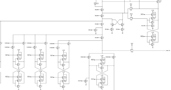
For flash memory, waveform analysis provides details of the programming algorithm and measurements on the internally generated voltages required to program, read, and erase memory cells during various device operations and modes. The memory is tested in an active probe arrangement , and voltage traces of the selected signals are recorded during device operations.
Our waveform analysis involves internal signal probing of targeted signals to interpret circuit functionality and system algorithms, including:
- Flash memory programming algorithms required to program, read and erase the memory /storage device
- CMOS image sensor pixel operation algorithms for sensing and reading out image
- DRAM data path operation and timing
Project flow main steps
1. Circuit Extraction
2. Package Analysis (Decapsulation & Modification)
3. Flash Programmer and External Functional Testing
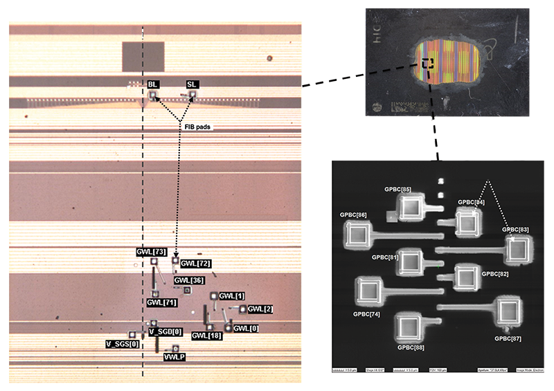
4. Probe Pad Placements (FIB)
5. Waveform Captures and Analysis
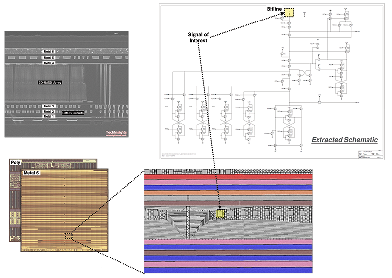
1. Circuit extraction
The extracted schematic(s) are typically part of an already completed circuit report (CAR) of the same device/die. If no CAR is readily available, circuit extraction of the area(s) of interest is first required to identify the signals of interest on the layout and to determine if accessible.
Learn more about our circuit extraction.
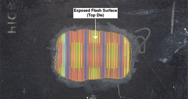
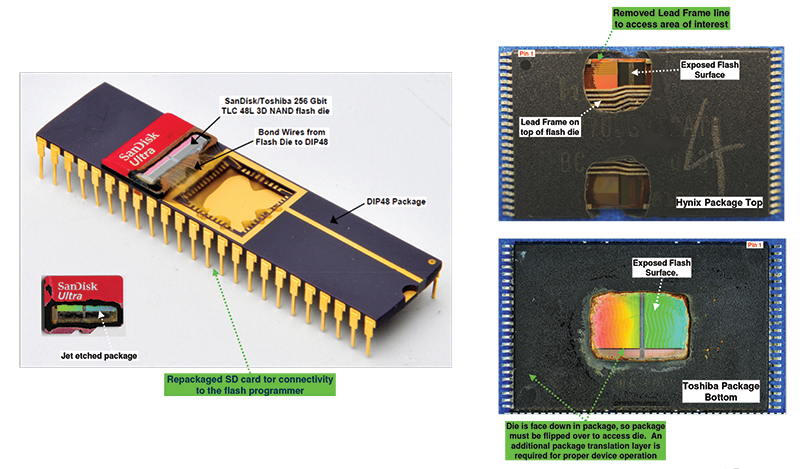
2. Package analysis
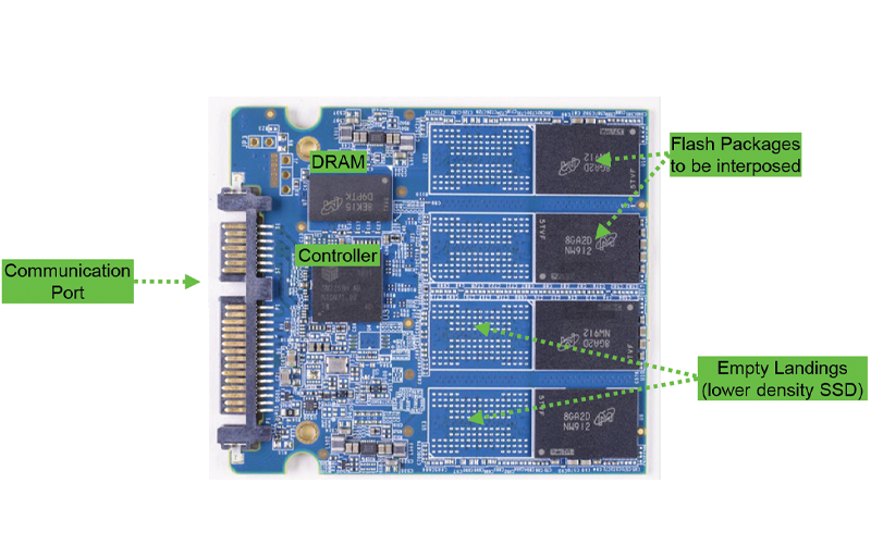
Decapsulation: Jet etch the memory package to expose a section of the die surface for probe pad placements
Some package challenges include: die obstructions, die orientation, die repackaging for standard NAND interface package connectivity to flash programmer
Learn more about our package analysis.
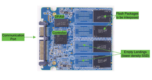
3. Flash programmer and external functional testing
Various flash programmer units are used to operate the NAND and NOR flash memory packages in various modes of operations such as asynchronous, multi-plane, specific vendor commands, etc…
For NAND flash, the commands and addressing may vary from device to device (for example the number of pages per block, wordline addressing vs page addressing, TLC vs MLC, commands prefix, etc…), so device datasheets is the quickest method for acquiring this information to generate the proper flash programmer driver based on the datasheets
If the device datasheets is not publicly available, then external functional testing to interpose the flash package within the memory system (such as SSD, phone, SD card) for connectivity to a logic analyzer to capture the communications between the controller and the NAND flash device during system operations to determine the commands and addressing methods required to operate the device.
The acquired and analysed commands and addressing information from the external functional testing is then used to generate proper flash programmer driver to operate the target NAND flash device
Learn more about our functional testing.
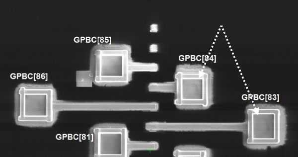
4. Probe pad placements (FIB)
FIB pad placement challenges includes:
- Smaller process nodes in current NAND flash
- Metallization material, thickness and width
- Bitline access on lower metals and line pitch in NAND flash to FIB the BL signals (may require additional FIB edits)
- Lower metal signals on M2 and M1 are difficult to FIB (back side FIB maybe an option) on array over CMOS type 3D-NAND devices
Learn more about our functional testing.
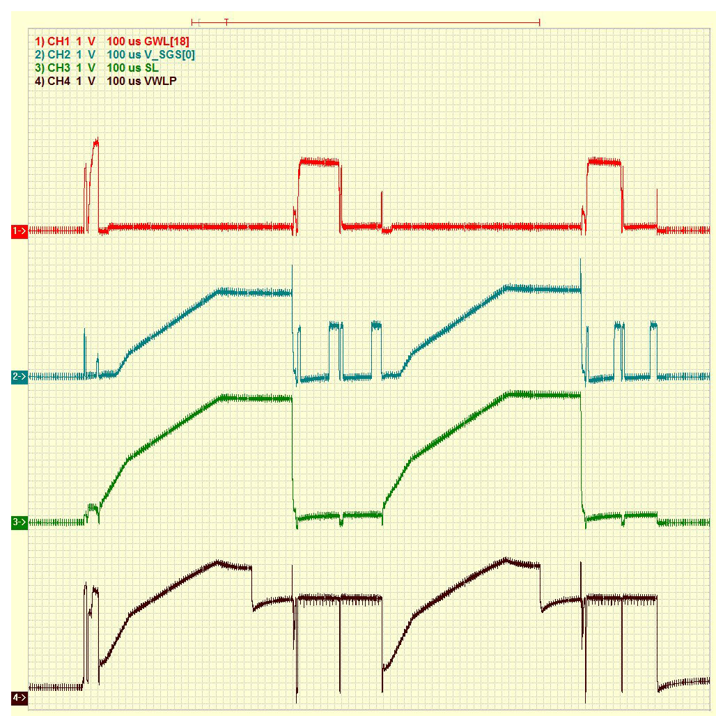
5. Waveform captures and analysis
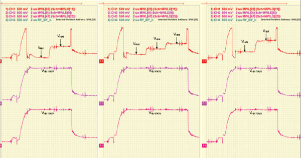
Two types of NAND internal WAR deliverables: Standard reportand custom report.
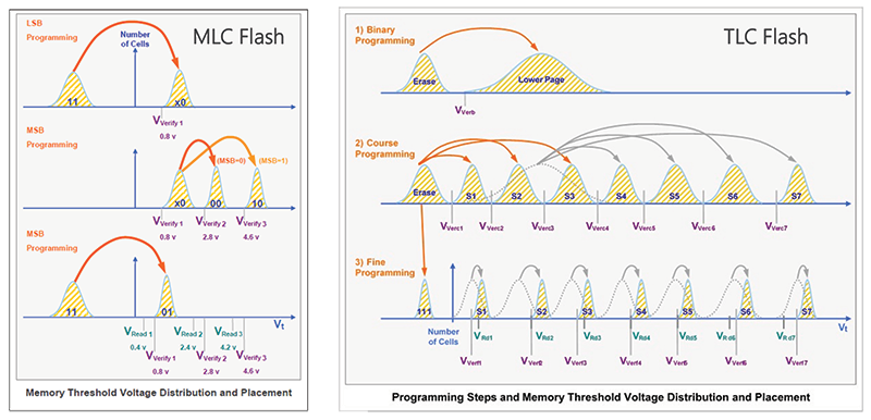
Standard reports include a pre-defined set of signals such as wordline, bitline, sourceline, PWELL, etc… (~10 signals total). The report will include all of the program, read and erase waveforms for all the memory states for the NAND device, so for example in TLC devices state 000 to state 111, tabulated voltages and a summary diagram of the state distribution
Custom reports can include as many signals as required by the client, so for example all of the signals on the page buffer circuit to understand the circuit operation by analysing the applied voltages and timings of the signals.
Custom reports can also include the program, read and erase waveforms and any other additional requests as needed to support their needs
All reports will optionally include the raw data sheet files for all the waveform figures with a viewer application as part of the final deliverable. The raw data sheet files allow the user to open each waveform figure and custom select the time scale, voltage scale and waveform colors as needed
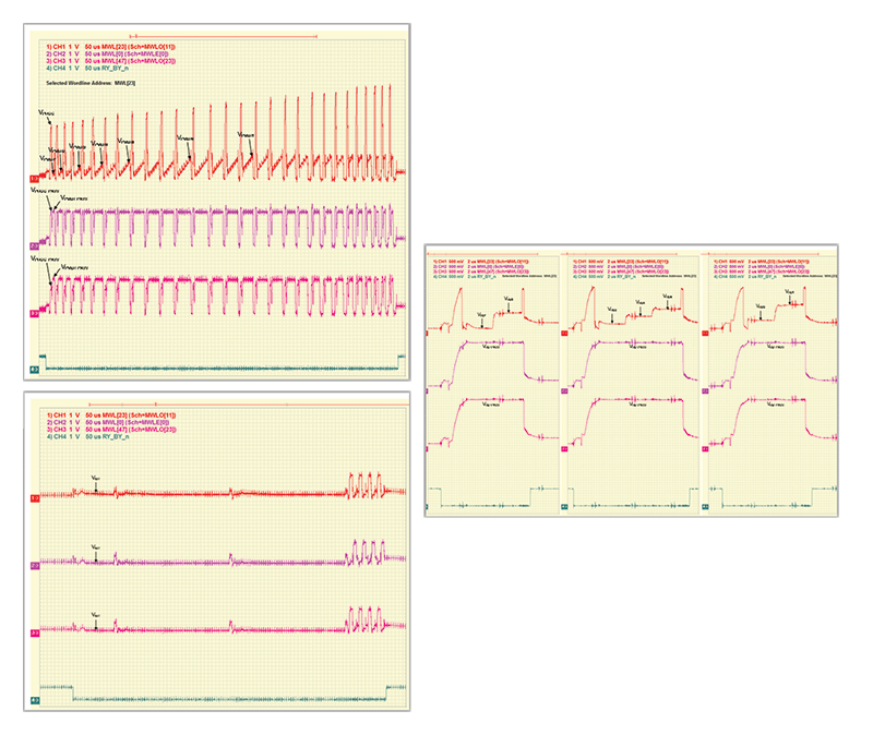
The captured waveforms for the program, read and erase operations in 3D- NAND flash for example as shown below provides details on the program algorithms of the tested devices for either patent related infringement analysis or for just understanding the latest on other vendors designs/solutions.
In standard type internal waveforms analysis, a memory threshold voltage distribution is also provided as a summary of how the different memory states (4 states for MLC devices and 8 states for TLC devices) are programmed and distributed as shown in the two examples below:
TIPS Webinar: Techniques to Analyze NAND Flash and SSD Devices - Internal Probing, Waveform Analysis, and More
This presentation examines some of the areas of innovation in NAND Flash and SSD devices and provides an overview of the various testing methods we apply to analyze these innovations.
Our Value
By revealing the innovation others can’t inside advanced technology, we prove patent value and drive the best IP and technology investment decisions.
Technical and product teams for the world’s most innovative and disruptive technology companies use our insights to make the best technology investment decisions.
By combining deep patent knowledge with the most advanced reverse engineering and technical analysis capabilities in the world we have demonstrated an unrivaled ability to match patents to products and deliver solid evidence of use in advance technology markets.
Our Analysis
Our analysis reveals the use of technology implementation in electronic circuits, software and manufacturing processes. They are used to gain intelligence about technology innovations and find evidence of use, proving patent value to technology, legal and patent professionals.

Get critical insight into innovations
We use state-of-the-art facilities, proprietary tools, and highly experienced technicians and engineers to reveal the inner workings and secrets of consumer electronics devices.

Apple M5 Pro Package Analysis: TSMC's SoIC-X F2F Hybrid Bonding in Consumer Computing
TechInsights analyzes the Apple M5 Pro APL1X15 package, revealing TSMC SoIC-X F2F hybrid bonding, CPU and GPU chiplets, silicon interposer routing, and verified die costs.

Why the AI Memory Shortage Could Keep DRAM and NAND Prices High for Years
AI-driven demand is creating the biggest memory shortage in history. Discover why DRAM and NAND prices are expected to remain elevated through the rest of the decade.

DRAM Market Update Q2 2026: Why This Cycle Looks Different
Stronger-than-expected demand, rising AI memory requirements, evolving procurement models, and record profitability are transforming the DRAM market in ways that differ from those of previous cycles.
![]()
The Authoritative Information Platform to the Semiconductor Industry.

