The optoelectronics market is expected to grow at a CAGR of 10.25% over the forecast period (2018-2023), fueled by growing demand for consumer electronic devices with advanced features and technological advancement. Consumer electronic devices, digital imaging solution and communication network are the major areas where Optoelectronics has market opportunity for its major High-brightness LEDs (HB-LEDs), CMOS image sensors and Fiber-optic laser transmitters components.
In addition to this, increased demand for advanced technology in automotive industry is creating market opportunity for Optoelectronics. Most of the automotive vendors are integrating infrared components in cars for detect ambient light, whether estimation, gestured control for the infotainment console and night vision. These new application areas strengthen the Optoelectronics market share in emerging sectors.
Areas of application for optoelectronic devices include image sensors, LIDAR, and LED lighting. Optoelectronic devices are foreseen to replace traditional electronics by surpassing the contemporary expedients in cost, performance, and consistency.
Recent innovations in optoelectronics field such as inexpensive 3D imaging, plasmanic nanostructures, perovskite transistors, optically active quantum dots, microscopic light bulbs, laser-powered 3D display technology, and Laser Li-Fi are anticipated to bring about a quantum shift in dynamic applicability areas of optoelectronic equipment.
Our Value
By revealing the innovation others can’t inside advanced technology, we prove patent value and drive the best IP and technology investment decisions.
Technical and product teams for the world’s most innovative and disruptive technology companies use our insights to make the best technology investment decisions.
By combining deep patent knowledge with the most advanced reverse engineering and technical analysis capabilities in the world we have demonstrated an unrivaled ability to match patents to products and deliver solid evidence of use in advance technology markets.
Our Analysis
Our analysis spans major market players such as:
- Avago
- Fujitsu
- Sharp
- Toshiba
- Panasonic
- Philips
- Omnivison
- Osram
- Sony
- Samsung
- Rohm
- General Electric Company
- On Semiconductors
- Mitsubishi
- Cree
- Finisar
- JDSU
Our state-of-the-art reverse engineering facilities have the unique ability to go from the system to atomic level
- Product Teardowns & Costing/BOM
- Functional testing
- Packaging Analysis
- Structural/Process Analysis (Structure, Material, Packaging etc.)
- Circuit Analysis
- Software Analysis
The Trusted Technical Intelligence Provider
TechInsights has been at the forefront of image sensor competitive technical intelligence since 2006, and have always been the first to report on key technology elements. All Top 10 image sensor design companies are our subscribers, and all Top 3 image sensor foundries are our subscribers.

Google I/O 2026: Gemini for Home Takes Center Stage
Google I/O 2026 focused on Gemini for Home, AI-powered smart devices, and agentic AI, signaling a software-first future for the smart home market.
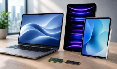
PC and Tablet Market Trends | AI PCs, Apple M5 & Memory Costs
Discover the latest PC and tablet market trends, including AI PCs, Apple M5 devices, Intel Panther Lake, processor forecasts, tablet market share, and the impact of rising memory costs.
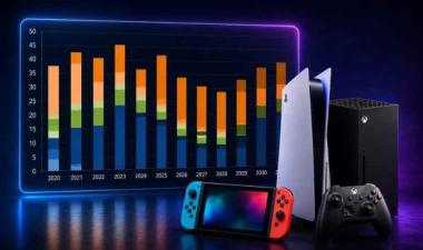
Game Console Forecast 2030: Rising Prices, Declining Shipments, and the Future of Gaming
Discover why rising memory costs, higher console prices, and longer upgrade cycles are expected to slow game console shipments through 2030. Explore the outlook for Nintendo Switch 2, PlayStation, and Xbox in the latest TechInsights forecast.
![]()
The Authoritative Information Platform to the Semiconductor Industry.

