eBook:
The state of the art of CMOS image sensors
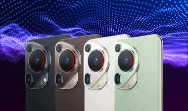
CMOS image sensors (CIS) have continued to evolve in response to performance requirements of current applications of Smartphone Imaging, Security Surveillance, Biometrics, Automotive and Depth Sensing and Ranging.
Get regular, succinct analysis of high-volume and emerging imaging and optical sensing applications
For leaders who want to base their product road maps on hard facts and understand what’s really going on under the hood of state-of-the-art imaging devices, TechInsights' Image Sensor subscription is the ideal solution.
We have created an eBook based on a presentation given at IISW 2021 by Ziad Shukri, a TechInsights Subject Matter Expert in Image Sensors.
Download “The state of the art of CMOS image sensors” to learn about:
- the latest analysis and trends of CMOS image sensors - resolution, pixel pitch, chip stacking and die configuration
- active silicon thickness and pixel aspect ratio trends
- trends and comparative analysis on Time-of-Flight (ToF) sensors, including both Front- and Back-illuminated, as well as recent Near-Infrared (NIR) -optimized sensors
- CIS trends for emerging applications and the challenges that lie ahead
eBook table of contents
- Introduction
- Configuration & Die Size
Learn about trends in CIS configuration from 2011 to 2020; front-illuminated (FI), back-illuminated (BI) and back-illuminated-stacked, and the ratio of active CIS area to total CIS area - Pixel-Pitch & Active Silicon
See the trend of silicon thickness and the ratio of thickness to pixel-pitch, and detailed images of the Samsung GW3 and Omnivision’s OV64B - Phase Detection Auto Focus
Presents a comparison of PDAF methods for smartphone imagers in terms of resolution and pixel-pitch. This chapter includes detailed image examples of masked PDAF, on-chip lens (OCL), and dual photodiode (DP) - Color Filter Array
Maps the color filter array (CFA) trends of Bayer, Tetracell, Quad Bayer, 4-cell, Nonacell, and 4x4 Bayer CFA patterns; compares the approaches of Samsung, Sony, and OmniVision - Chip Stacking and Pixel-Level DBI
Maps the trend of DBI pitch for Cu-Cu Hybrid bonding for all stacked images analyzed between 2014 and 2021, provides detailed images of examples from OmniVision and Sony - Near-Infrared (IFR) Enhancement
Shows the trend of active silicon thickness for back-illuminated imagers by application (automotive, depth sensing, machine vision, mobile, security and surveillance, and linear; image examples are provided for back-surface with NIR-enhancement with inverted pyramid arrays (IPA) for Sony, OmniVision, ON Semiconductor and Samsung - Time-of-Flight (ToF)
Discusses the ToF trend in terms of resolution (pixel count) from 2013 to 2022; examines the trend toward smaller pixels as the move toward back-illuminated imagers continues - Transistors Per Pixel
Examines pixel complexity per application – automotive, depth sensing, DSLR / MILC, event based sensor, machine vision, mobile, security & surveillance between 2009 and 2022
Find content like this and more in the TechInsights Platform. Sign-up for free today.