Webinar Follow up
Dr. Stephen Russell answers your webinar questions

Stephen Russell
I thoroughly enjoyed our recent gallium nitride (GaN) focused webinar ‘Recent GaN Innovation: Moving from Consumer to Data Center and Automotive’ which is still available on demand at any time. There were some great questions that were asked in our Webinar Q&A and, I am answering them here today.
Q: Is there a place for GaN below 40 V?
A: There is a large market already available to GaN in consumer electronics. 650 V GaN HEMTs are increasingly found in USB chargers, more recently they are also being used in datacenters for primary side conversion. 40 V and 100 V GaN devices are increasingly making inroads in secondary side DC-DC conversion for 12 V and the increasingly popular 48 V distribution regime, respectively. These low-voltage devices also have further applications in which GaN can offer unique benefits, such as laser driving for LiDAR applications or low-voltage DC motors.
Could GaN go even further and unseat silicon for final stage point of load (PoL) conversion inside the consumer device itself? There is no theoretical reason this could not happen, there are however, some practical reasons that make this particularly challenging.
Like any electronic device, the GaN HEMT can be broken down into regions of resistance. The utilization of a two-dimensional electron gas (2DEG) arising from the heterojunction nature of the device gives low transistor channel and ‘access’ resistances. These will also scale to an extent with voltage as the device dimensions decrease. Source and drain contact resistance unfortunately do not, they will essentially be the same for a 650 V and a 40 V device. At 650 V they are relatively insignificant but as dimensions decrease, they become far more pronounced.
It seems to date 40 V is the ‘sweet-spot’ where this trade-off still makes sense, below which silicon is still the more practical solution. 40 V are the lowest GaN based device we have analyzed at TechInsights. Both Efficient Power Conversion’s EPC1015 and EPC21601 are examples of this. The cell pitch of the GaN HEMT array shown in Figure 1 is over 6x smaller than 650 V devices we have reported on.
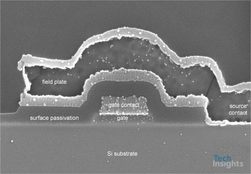
Figure 1. EPC21601 GaN HEMT source & gate region
It is also worth remembering that as dimensions decrease capacitances will also become more pronounced. This is of note when wanting to operate a device at high frequency – one of the selling points of GaN products.
There is definite interest in pursuing these lower voltages. Some companies have even announced <40 V GaN prototypes, Innoscience for example recently presented a 15 V GaN HEMT prototype with an on-resistance * gate charge figure of merit of 13.1 mΩ.nC at this year’s International Symposium on Power Semiconductor Devices. We have observed an increasing trend for analog component integration in GaN products, perhaps one day we may be discussing true GaN power management integrated circuits (PMICs).
Q: Will vertical GaN devices be a market disruptor?
A: Vertical GaN FETs have seen intense academic research over recent years. Firstly, it is worth defining what exactly we mean by a vertical FET.
Figure 2 shows a simplified version of the lateral GaN HEMTs we see in the market today, note the GaN in all these devices is a heteroepitaxial layer grown on a carrier substrate. Silicon is the most common, although silicon carbide (SiC) and sapphire are also used.
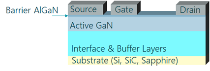
Figure 2. Simplified layout of a lateral GaN HEMT
The growth of freestanding GaN wafers is possible, but expensive and large area substrates are still in their infancy. One method to get around this is a ‘quasi-vertical’ structure. A quasi-vertical JFET is shown in Figure 3 (diodes or even MOSFETs could also be made via this method in theory). This uses a slightly different arrangement of GaN epitaxy but still needing a carrier substrate. The bottom drain contact is made on a highly doped contact layer which extends beneath the device.
This method has been popular in academic research to demonstrate the promise of vertical GaN devices, yet the device area required is large. This, and the necessity of deep GaN etches make it impractical from a production standpoint.
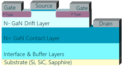
Figure 3. A quasi-vertical GaN JFET
A truly vertical GaN device (similar in structure to a traditional Si power FET or SiC FET) requires a freestanding GaN substrate as seen in Figure 4. The material growth, quality, and cost remain the largest challenge to product realization. Because of these factors, commercial devices are some way off, mass production is unlikely until 2030 at the earliest.
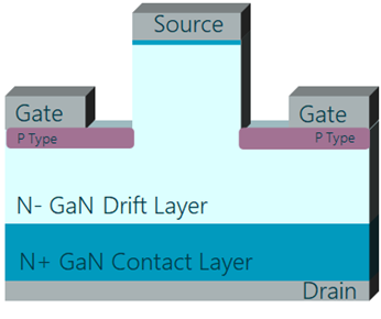
Figure 4. A Vertical GaN JFET
A company pursuing the approach shown in Figure 4 is NexGeN Power Systems. Their website boasts operation from ~40 V to over 4 kV with frequency performance up to 10 MHz and avalanche capable. We will be keeping a close eye on their progress moving forward.
However, even these devices are JFETs. To achieve a true vertical GaN MOSFET would require further process developments.
- GaN lacks a native oxide (SiO based gate dielectrics can be thermally grown on both Si and SiC), so a high-quality deposited dielectric would be necessary.
- The JFETs discussed above can create a channel in the bulk GaN material which is pinched off by the P-type gate regions (likely epitaxially grown). The prospect of an implanted p-type body with precise dopant concentration control and where an inversion channel can be created is still daunting.
Why is there such interest in this approach? 650 V GaN HEMTs are seeing success in the consumer market and 1200 V devices are close behind. The lateral GaN HEMT structure fundamentally limits going higher in voltage while retaining a competitive die size. The bandgap of GaN is in fact marginally higher than that of SiC, so there is absolutely opportunity for GaN at this higher end of the power spectrum.
In conclusion
GaN is an outstanding material offering many benefits for power device manufacture. To date we have seen there is not a ‘one size fits all’ approach to power devices, hence why we see silicon, SiC and GaN all carving out their niches within the market. We expect this to remain the case for some time if not indefinitely, although each material manufacturer will certainly feel they can make inroads into other markets.
The processing of GaN will continue to see advancements while silicon is near its theoretical limit. With the cost of GaN devices continuing to reduce it seems inevitable inroad will eventually be made in to the < 40 V market. The challenges facing vertical devices are more significant, however the rewards could be even greater.
References
- Recent GaN Innovation, Moving from Consumer to Data Center and Automotive (TechInsights) 2022.
- Efficient Power Conversion EPC1015 Enhancement Mode GaN-on-Silicon Power Transistor Exploratory Analysis Report (EXR-1005-801) TechInsights, 2010.
- EPC 21601 40V, 10A eToF Laser Driver IC Power Floorplan Analysis (PFR-2104-801) TechInsights, 2021
- Navitas NV6128 650 V GaN Power Essentials (PEF-2104-802) TechInsights, 2021.
- Dynamic Rdson and Vth Free 15 V E-mode GaN HEMT Delivering Low sFOM of 13.1 mΩ•nC and over 90% Efficiency at 10 MHz for Buck Converter (ISPSD 2022 Proceedings) 2022.
- NexGen Vertical GaN™ Core Technology - Enabling a New Benchmark in Power Electronics (NexGen Power Systems Website) 2022.
- The Dawn of 1200 V Gallium Nitride Transistors (TechInsights) 2022.