Memory Blog
YMTC’s Xtacking 3.0 – Not what TechInsights was expecting to see
Contributing author: Chi Lim Tan
Yangtze Memory Technology Company (YMTC) has been making headlines since it was founded in 2016. Considered China’s leading Integrated Device Manufacturer (IDM) for NAND memory, YMTC has been moving fast. They first introduced their Xtacking 1.0 architecture at 2018’s Flash Memory Summit (FMS), quickly followed by Xtacking 2.0 in 2019.
As it has been for so many technology companies, 2022 has been a rollercoaster of a year for YMTC. First came widespread news of Apple’s plans to incorporate YMTC’s 128L chips into its products, then a rapid about-face when the US Government imposed restrictions on YMTC. In the midst of it all came YMTC’s press release that Xtacking 3.0 was now available, which brought questions around whether the company was still positioned to produce the device at scale without Apple’s continued backing.
TechInsights sees Xtacking 3.0 as one of the most disruptive technologies of 2022. First, the innovative architecture doesn’t really have a peer in the emerging memory semiconductor industry; second, the restrictions recently imposed on YMTC have thrust this technology into the geopolitical spotlight.
This week, TechInsights team received several units of the TiPlus7100 – the first device in which Xtacking 3.0 is supposed to be used. We were surprised by our findings.
What did TechInsights find?
According to YMTC’s press release about Xtacking 3.0, the technology can be found in every version of the TiPlus7100 high-speed SSD. TechInsights purchased the 512GB and the 1TB; the 2TB is not yet available for purchase.
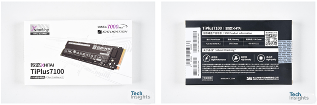
Figure 1. ZhiTai TiPlus7100 1 TB SSD Images
TechInsights has not yet found Xtacking 3.0 inside any of the models of the TiPlus7100 that we have torn down. The dies TechInsights has evaluated so far:
- Are 128L (Figure 5), not 232L
- Include a die layout of 2x2 plane (Figure 4), not 3x2 as YMTC has described
- Do not include Xtacking 3.0 features, such as the back side source connect (BSSC) or the center X-decoder.
Two 512 GB NAND packages (Figure 2) are found within the TiPlus7100 1 TB SSD. Two spare slots are available in the printed circuit board (PCB).
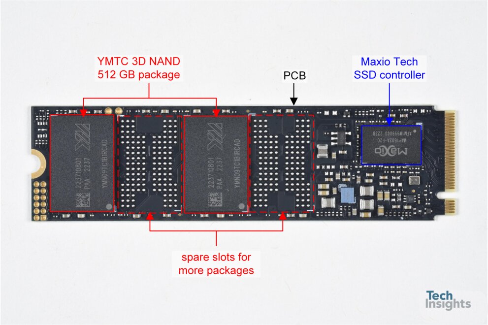
Figure 2. PCB image
The 132-pin ball grid array (BGA) multi-chip package (MCP) measured 18.0 mm × 12.0 mm × 0.9 mm (Figure 3). The package date code of week 37 of the year 2022, indicated the packaging was done in the September timeframe (not long after the debut of Xtacking 3.0 at Flash Memory Summit 2022).

Figure 3. YMTC NAND package images
There are eight NAND dies (die marking of CDT2A) within each NAND package. The CDT2A die has a layout of 2×2 plane (Figure 4). This is different from the previous YMTC 128L die layout [2] which had a 1x4 plane. TechInsights' analysis revealed that the new YMTC CDT2A die is in fact a YMTC 128-Layer 3D NAND, with total gates count of 141 (Figure 5).
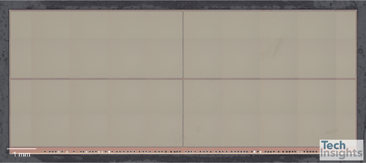
Figure 4. CDT2A Die Image
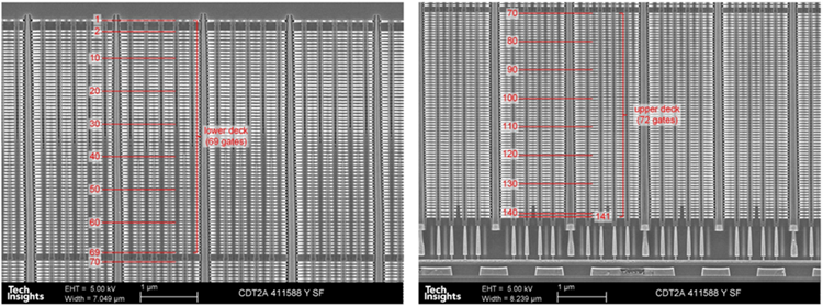
Figure 5. Cross-Sectional SEM images of Memory Array, lower (Left) and upper deck (Right)
Some news sources are speculating that YMTC may not have the funding, with Apple’s withdrawal, to produce Xtacking 3.0 in high quantities. It could be that TechInsights simply hasn’t been lucky enough in our search for parts to secure one of the few with true Xtacking 3.0.
TechInsights’ analysis continues – we are still digging deeper into the 512GB and the 1TB. It appears that the packages may include a mix of Xtacking 2.0 and 3.0. And our procurement efforts continue. If Xtacking 3.0 is out there, TechInsights will find it.
Evolution of Xtacking technology – what’s in Xtacking 3.0?
Xtacking is the registered trademark of YMTC for their innovative 3D NAND architecture that involves wafer bonding of a CMOS wafer and a memory cell wafer, as shown in Figure 6.
Interested in bonding technologies? Check out TechInsights’ upcoming webinar on Hybrid Bonding here.
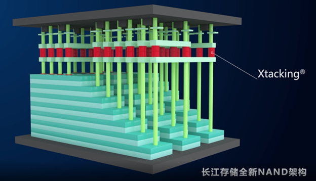
Figure 6. Xtacking, Source: YMTC
Major points of evolution from Xtacking 1.0 to what is reportedly included in Xtacking 3.0 can be summed up as follows:
- Xtacking 1.0 uses wafer to wafer bonding for higher cell efficiency and reduced development time.
- Xtacking 2.0 implements nickel silicide (NiSi) instead of tungsten silicide (WSi) for better device performance and I/O speed for CMOS wafer
- Xtacking 3.0 introduces back side source connect (BSSC) for memory cell wafer, which leads to simpler process and lower cost
At FMS 2022, YMTC spoke of the 1 Tb die X3-9070 (depicted in Figure 7), a chip that features six planes with asynchronous multi-plane independent (AMPI) operation per plane with center X-decoder (X-DEC); architecture that would allow a 50% increased speed with Xtacking 3.0.
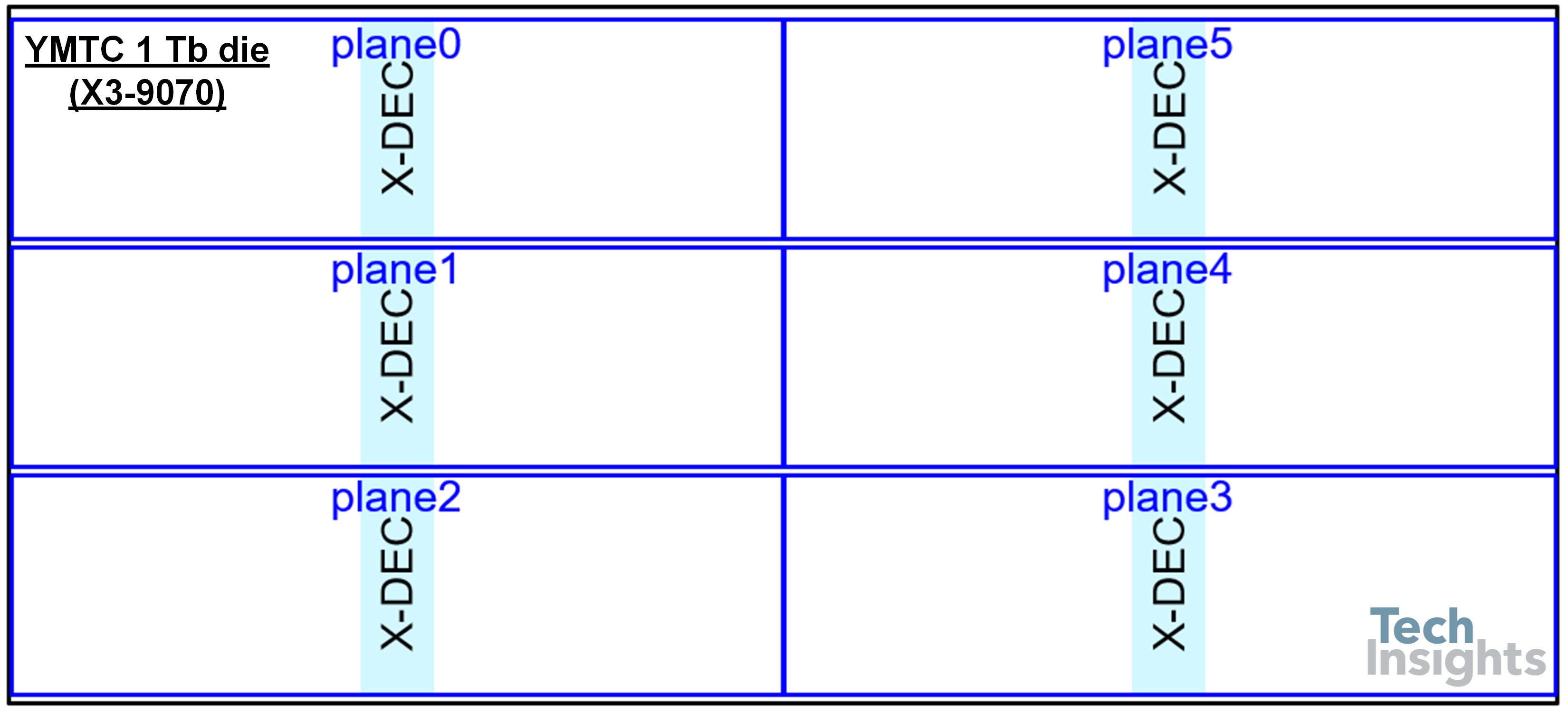
Figure 7. Representation of the YMTC 1 Tb die (X3-9070), discussed by YMTC at FMS 2022
With the BSSC implementation, YMTC is likely eliminating the challenging ONO etch (before Si channel deposition) and the costly selective epitaxial growth (SEG) Si. Figure 8 shows the expected changes between YMTC 64-L (with Xtacking 1.0) and YMTC 232-L (with Xtacking 3.0). There is also the possibility of material change for the bonding interface as Adeia (formerly Xperi) licenses their hybrid bonding technology to YMTC.
Note: TechInsights has comprehensive analysis on all of YMTC’s memory products released since 2016, including Xtacking 1.0 and Xtacking 2.0. Subscribers can access this data in the TechInsights Platform, other interested parties can reach out to TechInsights to request additional information.
It is common knowledge that Xtacking 3.0 will be found in a 232L die. The large parasitic capacitance of the 232L stacked WL structure causes performance degradation. To counter this degradation, the center-XDEC design cuts the WL capacitance in half and reduces the RC load and RC delay (tRC) compared with edge-XDEC. Center-XDEC design can reduce the WL settling time and the current required to charge the WL. By adopting the center-XDEC, the performance can be increased by 15~20% compared to the previous edge-XDEC. For these reasons, TechInsights is sure that the center-XDEC will be the mainstream of the 3D NAND die design.
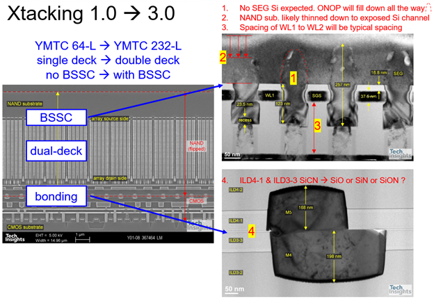
Figure 8. Images showing features of Xtacking 1.0 (64-L), with notes indicating expected changes from Xtacking 1.0 to Xtacking 3.0 (232-L)
Other memory related features/processes of Xtacking 3.0 are expected to be similar to those found in YMTC 128-L (Xtacking 2.0), as shown in Figure 9.
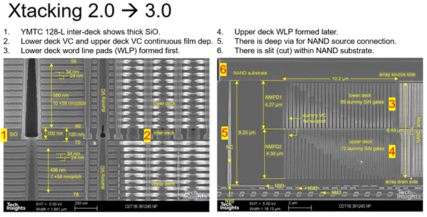
Figure 9. Images showing features of Xtacking 2.0 (128-L), with notes indicated where changes are not likely to be expected, from Xtacking 2.0 to Xtacking 3.0 (232-L)