Memory Blog
YMTC 232L Xtacking3.0
Now, YMTC is a Leading Pioneer in 3D NAND
Jeongdong Choe
March 02, 2023
A note from the editor:
Dr. Jeongdong Choe penned the following article in December 2022. Technology moves quickly – here we are in March 2023, and it has just been announced that YMTC has received a huge cash infusion of $7 billion USD. We have also just received the Micron 232L NAND SSD, and will be reporting our findings shortly.
Share This Post
Jeongdong Choe
Senior Technical Fellow, TechInsights
Dec. 2022
Chinese NAND champion Yangtze Memory Technologies Corp’s (YMTC's) recent remarkable growth and technological prowess took many of us by surprise. I am quite curious as to where and how they got their superpowers. In 2016, when YMTC announced that it would enter the 3D NAND business, six front runners including NAND veterans Samsung, SK Hynix, Micron, Toshiba, Western Digital (WD), and Intel, were already running the race; it seemed that if YMTC did jump into the 3D NAND world, it could only hope to rank 7th. In addition to market position, YMTC faced other challenges such as process, device, design, and circuit technologies in the early stages of starting a new NAND business, and a lack of experience in mass production as well.
At that time, it was predicted that even if YMTC could occupy part of the domestic market in China, 3D NAND would not be their future, and it would instead make products applicable only to low-level applications such as some of the domestic secure USB devices in China.
However, I would say this prediction was completely wrong. Since 2016, YMTC has successfully developed higher-density 3D NAND SSD products by combining their own process and design technologies based on Xtacking Hybrid bonding technology. Here, ‘X’ in Xtacking is from the first letter of the company, XMC. Now, by skipping the release of a 176-layer solution, YMTC has jumped directly into developing and mass-producing the 232-layer Xtacking3.0, which is the first 200+ layer solution we’ve found on the market. It’s the most advanced product with the highest bit density and the highest number of layers ever in the 3D NAND field.
Given that Micron just started to ship 232L NAND SSD for PCs and laptops, Samsung has successfully developed 232L custom samples, and SK Hynix’s 238L development is ongoing now, YMTC’s new 232L Xtacking3.0 TLC technology is a disruptive one and it may lead the future of 3D NAND technology.
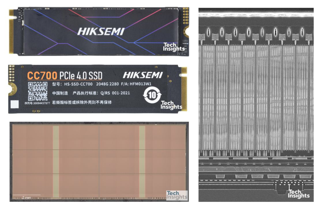
Figure 1. HIKSEMI CC700 PCIe 4.0 2TB SSD, YMTC Xtacking3.0 232L 1Tb TLC die, and 3D NAND array/Periphery X-section SEM images, TechInsights 2022
Compared to the 112-layer mass production and 162-layer prototype development stage of KIOXIA (previously Toshiba Memory), the founder of NAND that was developing and mass-producing on par with Samsung in the early days of 3D NAND, YMTC is already more than one generation ahead where they had previously been trailing 12 months behind their closest competitors. Moreover, YMTC made and commercialized products with more than 200 layers in just seven years, from and including 2016. Since the first 3D NAND prototypes from Samsung (TCAT V-NAND) and Toshiba (BiCS structure) introduced in 2007, the development and mass production of 2xx layer 3D NAND has taken more than 15 years. That being said, YMTC 232L Xtacking3.0 commercial SSD products are quite meaningful and represent remarkable technological growth. Where do the driving force and momentum of YMTC come from?
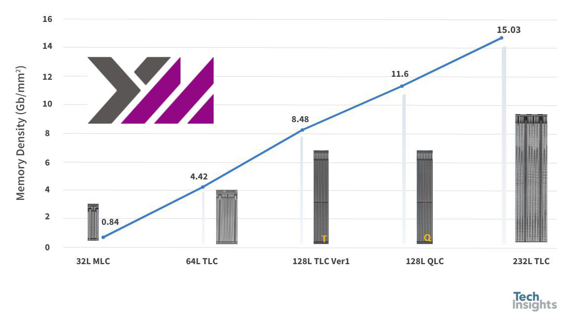
Figure 2. YMTC 3D NAND bit density trend, Gen1 through Gen4, TechInsights 2022
Let's take a quick look at YMTC's recently shipped 232L Xtacking3.0 SSD product here. The product with YMTC 232L chip is the HIKSEMI CC700 PCIe 4.0 2TB SSD, and the Xtacking3.0 chip consists of eight 1Tb dies stacked in a device package (Figure 1). The bit density increased by 76% from the previous 128L TLC second version Xtacking2.0 512Gb die (Figure 1), and the total number of vertical gates counted 253 (Figure 2).
Now, the bit density of NAND has exceeded 15.0 Gb/mm2 even with TLC products instead of QLC ones. For reference, the Micron 176L QLC N48R die has 14.9 Gb/mm2 density and 14.6 Gb/mm2 for the 232L TLC chip. Considering that the total number of vertical gates is 253, the vertical cell efficiency exceeded 91.6%. These figures show quite a difference in technology compared to the current 176-layer mass-products from leading companies Samsung, Micron, and SK Hynix. It should be noted that Micron was the first to announce 232L 3D NAND products last August, and Samsung recently started to ship 236L sample products, but TechInsights has not yet been able to find these products in the open market. The YMTC 232L Xtacking3.0 SSD products we purchased and analyzed show that YMTC's 3D NAND technology and productivity have risen considerably.
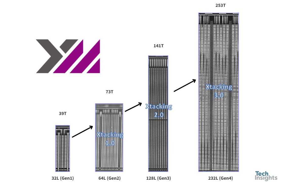
Figure 3. YMTC 3D NAND cell structure, Gen1 32L through Gen4 232L (x-sectioned SEM images in BL direction), TechInsights 2022
A comparison of YMTC's 3D NAND technology by generation can be seen in Table 1. The first baby product of YMTC's 3D NAND had a 32-layer structure and was not much different in structure and process from Samsung TCAT V-NAND which was mass-produced by Samsung at the time. However, YMTC did not focus long on the mass-production of 32-layer products, and instead skipped right over 48-layer products and jumped to developing 64-layer products. They introduced an Xtacking technology in which H-bonding with two wafers, a NAND wafer and a peripheral logic circuitry wafer, were used. NAND and logic wafers are separately processed and attached, followed by TAC and BEOL. The Xtacking technology was the world-first applied to memory devices, and YMTC successfully entered the high-density and high-performance 3D NAND market. Since then, they skipped 96-layer products and succeeded in mass-producing 128-layer Xtacking2.0 in which some of the innovations such as new material for the gates (NiSi) and a 2-deck process were applied to secure their reputation for technological prowess.
| Items | YMTC 3D NAND Gen1 (32L MLC) | YMTC 3D NAND Gen2 (64L TLC) | YMTC 3D NAND Gen3 (128L TLC, 1B-Die) | YMTC 3D NAND Gen4 (232L TLC) |
|---|---|---|---|---|
| Parent Product (Example) | 32 GB Secure USB | Gloway YCT512GS3-S7 Pro 512GB SSD |
Asgard PC!e4.0 NVMe1.4 AN4 1TB SSD |
HIKSEMI CC700 PCIe 4.0 2TB SSD |
| Package Markings | YMEC6A1MA3A2C1 | YMN08TB1BHU1B | YMN09TC1B1HC6C | YMC6G008Tb78DA1C0 |
| Memory/Device | 256 Gb | 1 Tb | 2 Tb | 8 Tb |
| Die Markings | 98081A | BCT1B | CDT1B | EET1A |
| Architecture | T-CAT | Xtacking1.0 | Xtacking2.0 | Xtacking3.0 |
| # Dice, Memory/Die | 4, 64 Gb | 4, 256 Gb | 4, 512 Gb | 8, 1 Tb |
| Die Size | 76.30 mm2 | 57.96 mm2 | 60.42 mm2 | 68.15 mm2 |
| Memory Density | 0.84 Gb/mm2 | 4.42 Gb/mm2 | 8.48 Gb/mm2 | 15.03 Gb/mm2 |
| # Planes | 1 | 2 | 4 | 6 (Center-XDEC) |
| # Decks, # Gates | 1, 39T | 1, 73T | 1, 141T (69 + 72) | 2, 253T (128 + 125) |
| Vertical Cell Efficiency | 82.1% | 87.7% | 90.8% | 91.7% |
| # Metals | 3 | 8 | 11 | 11 (BSSC) |
| Channel Hole Height | 2.74 µm | 4.14 µm | 8.49 µm | 12.0 µm |
| WL Pitch (Z-direction, min.) | 70 nm | 58 nm | 58 nm | 48 nm |
| BL Pitch | 39 nm | 39 nm | 39 nm | 39 nm |
| Unit Cell Area | 0.018 µm2 | 0.021 µm2 | 0.021 µm2 | 0.021 µm2 |
Table 1. A comparison of YMTC 3D NAND devices; Gen1 (32L) through Gen4 (232L), TechInsights 2022
Driven by that momentum, now, ahead of other companies, YMTC has commercialized SSD products using 232L Xtacking3.0 technology. It would not be an exaggeration to say that YMTC is now one of the leading companies in 3D NAND technology. Looking at the NAND cell array of YMTC's Xtacking3.0 chip, the new BSSC (Backside Source Connect) technology is applied to simplify the source connection process, and the cost and throughput are significantly improved by removing the interlayer between decks (Figure 4). Further, the new Xtacking3.0 1Tb die uses a center-XDEC which improves NAND operation speed compared to the previous edge-XDEC.
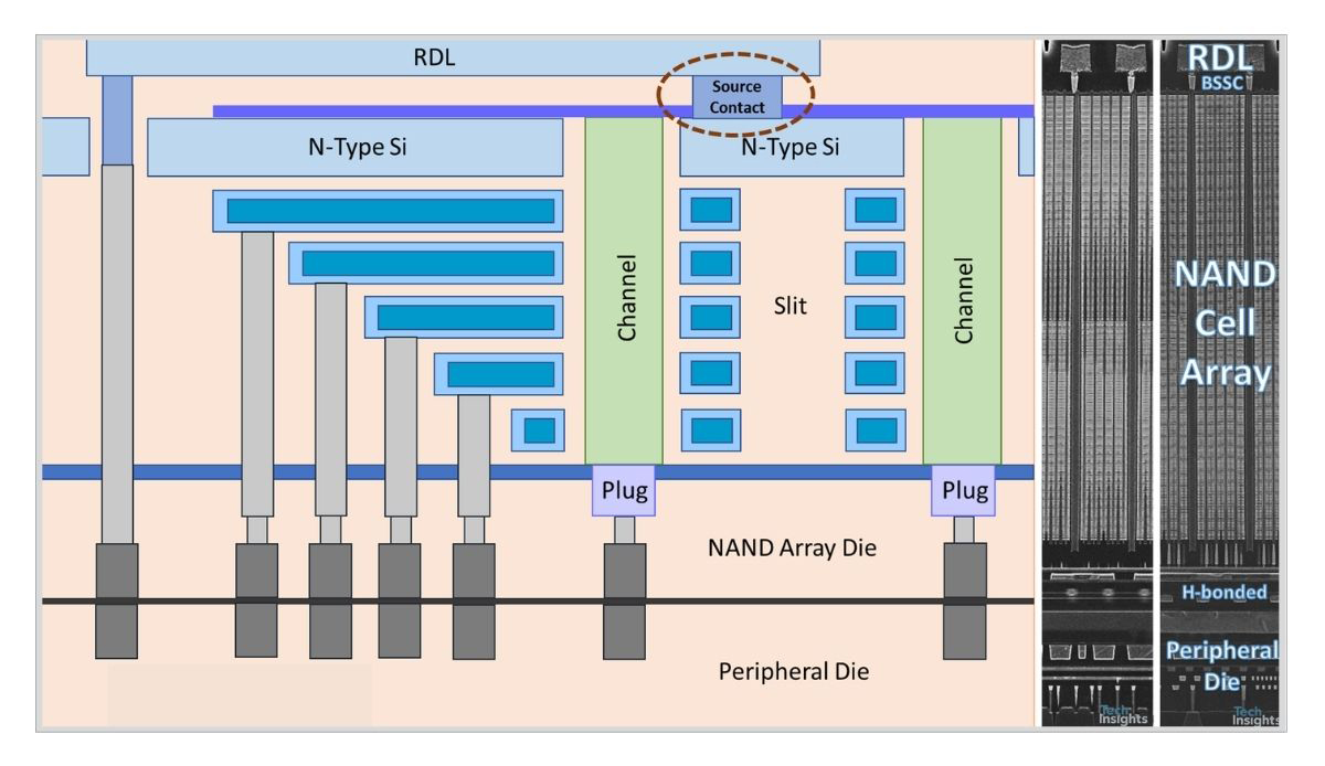
Figure 4. YMTC’s newly adopted BSSC (Backside Source Connect) structure for Xtacking3.0, TechInsights 2022
YMTC’s fairytale 3D NAND story has a few background factors to consider. The Chinese government's strong investment into and encouragement of YMTC took much of the cost risk out of R&D, highly skilled hard-working engineers in YMTC and experienced and skilled engineers contributed from external organizations, the timely investment into and securing of Fabs, and management of YMTC's supply chain (HIKSEMI) are major drivers behind YMTC to get them to this point, and for YMTC to continue their tales of success. In addition, Western sanctions levied against several Chinese technology companies in recent years have further fueled China’s interests in becoming technologically independent. Unlike the Logic Foundry and DRAM business which have no choice but to use EUVL equipment from ASML and semiconductor equipment from US companies such as AMAT and LAM for future advanced generations such as FinFET, GAA, MBCFET, and nanowire, 3D NAND processes do not use EUVL equipment. It is expected that Chinese independent technological prowess and preemption of the next-generation 3D NAND products will continue for the time being.
YMTC’s main cause for concern is that the commercial market for their 3D NAND products is mostly limited to mainland China. Most of YMTC's Xtacking products have been used for secure, SSD, and USB applications which are used only in China. Recently, YMTC 3D NAND chips have started to be used for some Chinese smartphone products. For example, TechInsights confirmed YMTC 3D NAND chips were used in Huawei Mate Xs 2 foldable phones.
Only 15 years ago, the question was whether or not 3D NAND could be commercialized. 5 years ago, people questioned whether 3D NAND products could exceed 200 layers due to technical limitations such as wafer warpage, cell current, and HAR. However, today we have seen SSD products with over 200 layers in the open market. Now, our question has changed to whether NAND products and technologies will exceed 1,000 layers. The technological challenges for the next 3D NAND generations will be overcome and resolved in the future, and it is expected that this will lead to the advancement of higher memory density, higher speed, and higher bandwidth memory technology along with hybrid-bonding, package solution, and CXL interface technology. From where I sit, it looks like YMTC will continue to be among the leaders as 3D NAND continues to evolve.
Make informed business decisions faster and with greater confidence
Gain sample access to the world’s most trusted source of actionable, in-depth intelligence related to semiconductor innovation and surrounding markets.


